Proper RC Snubber Design
When switching high currents through external power MOSFETs to commutate a BLDC motor, ringing can occur, leading to concerns in electromagnetic interference (EMI), circuit jitter, excessive power dissipation, and overstressing components. This is often due to parasitic inductances and capacitances in the Printed Circuit Board (PCB), specifically in the high-current-carrying phase nets between the high-side and low-side MOSFETs. Inductors and capacitors form an inductor-capacitor (L-C) tank circuit, resulting in resonance during switching events.

Figure 1 – Ringing at motor phase output due to L-C tank resonance
In order to mitigate the ringing at the phase output, a simple resistor-capacitor (R-C) snubber circuit can be used to “snub”, or dampen the oscillations. By removing the oscillations, this will reduce potential EMI and increase the longevity of the MOSFETs by reducing voltage overstress. The R-C snubber is placed in parallel as close as possible to each MOSFET’s drain and source connections.
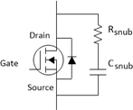
Figure 2 – RC Snubber
To calculate the resistor (Rsnub) and capacitor (Csnub) values of the R-C snubber circuit, we will use a 7-step procedure that shifts the resonant frequency of the MOSFET ringing to calculate the circuit’s parasitic capacitance (C0) and inductance (L). Once those are known, they will be used to derive the values of the R-C snubber. The example shown uses the RC snubber next to the CSD18540Q5B MOSFETs (Qgd = 6.8nC) of the DRV8343-Q1 EVM.
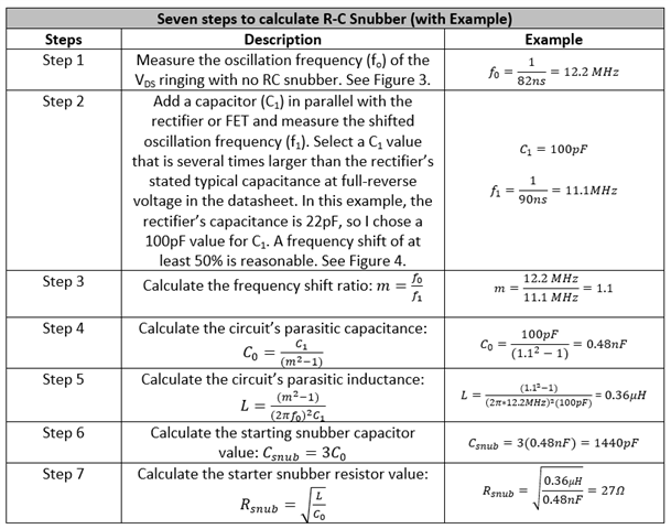
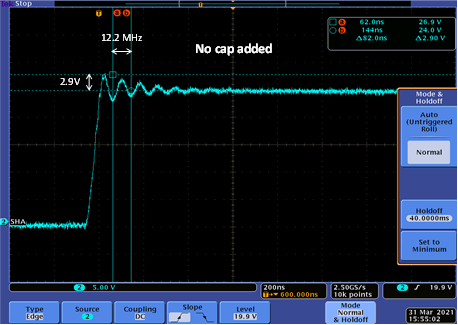
Figure 3 – Measure fo of VDS ringing without RC snubber
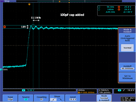
Figure 4 – Measure f1 of VDS ringing with C0 = 100pF
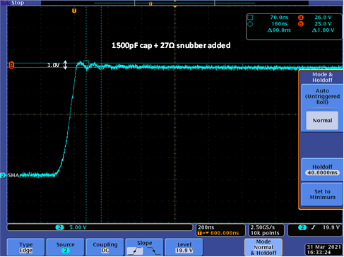
Figure 5 – MOSFET ringing is dampened using calculated RC snubber values
Figure 5 shows the spike reduction and damping effect of the calculated R-C snubber values. You can adjust the ringing higher or lower by varying the Csnub value. Larger values for Csnub reduce the voltage-spike amplitude further, but increase power loss in Rsnub.
Alternatively, you can decrease the power dissipation in Rsnub by lowering Csnub, but ringing will increase. You must weigh the trade-off between acceptable voltage-ring amplitude and Rsnub losses.
If a positive or negative voltage transient appears at the VDS switching event after snubbing out the ringing effects, you can lower the source current into the MOSFET gate or the sink current from the MOSFET gate. This will increase the rise and fall time of the MOSFET switching and reduce the maximum transient spike. It is important to monitor negative voltage transients when switching a MOSFET off to not exceed any maximum negative transient specifications of the gate driver device.

