Other Parts Discussed in Thread: DRV8316, DRV8301
Hi.
I'm working on TI's DRV8316REVM to control BLDC motor. And I use STM32G474RE(Nucleo board) as MCU to control DRV8316.
Now, I have issue that I can't read and write register of DRV8316 via SPI properly.
The situation is like this:
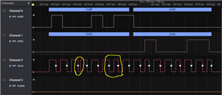
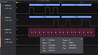
- SPI communication is OK, I believe so.
- After, power on, I read the default register values, but return values form the DRV8316 is not same value as datasheet. So, I think read operation is not OK.
ex.) I read Control3 register (address=0x05, reset value=0x00) and instead of 0x00 it was returned 0x46.
I saw the schematic, but I couldn't to find out any pin wiring for this register to return 0x46.
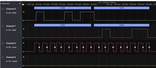
- Write to register and read it. The written value is not read. The return values of each register, is same as the operation 2. So, I think write operation is not OK.
My question about this issue is, any special initialization or communication rules need to read and write DRV8316 register?
Also I put a part of my test code.
Please let me know if any processing or settings are missing.
Test code for SPI:
static uint8_t getParity(uint8_t x)
{
uint8_t count = 0;
for (uint8_t i = 0; i < 8; i++)
{
count += (x >> i) & 0x01;
}
uint8_t parity;
if ((count % 2) == 0)
{
parity = 0;
}
else
{
parity = 1;
}
return parity;
}
int dev_drv8316_init(dev_drv8316_t *dev)
{
static volatile uint16_t timeout = 0;
int isTimeout = 0;
HAL_Delay(100);
HAL_GPIO_WritePin(DRV_nSLEEP_GPIO_Port, DRV_nSLEEP_Pin, GPIO_PIN_SET);
HAL_Delay(10);
HAL_GPIO_WritePin(DRV_OFF_GPIO_Port, DRV_OFF_Pin, GPIO_PIN_RESET);
HAL_Delay(10);
/**
* Read status registers during startup.
*/
DRV8316_ReadWordFormat_t rw;
while (1)
{
rw = dev_drv8316_read(dev, IC_STATUS_REG_ADDR);
dev->ic_status.data = rw.bit.data;
if (dev->ic_status.bit.FAULT == 0)
{
break;
}
if (++timeout > 999)
{
isTimeout = 1;
}
}
rw = dev_drv8316_read(dev, IC_STATUS_REG_ADDR);
dev->ic_status.data = rw.bit.data;
rw = dev_drv8316_read(dev, STATUS_1_REG_ADDR);
dev->status1.data = rw.bit.data;
rw = dev_drv8316_read(dev, STATUS_2_REG_ADDR);
dev->status1.data = rw.bit.data;
/**
* Read control registers.
*/
rw = dev_drv8316_read(dev, CONTROL_1_REG_ADDR);
dev->control1.data = rw.bit.data;
rw = dev_drv8316_read(dev, CONTROL_2_REG_ADDR);
dev->control2.data = rw.bit.data;
rw = dev_drv8316_read(dev, CONTROL_3_REG_ADDR);
dev->control3.data = rw.bit.data;
rw = dev_drv8316_read(dev, CONTROL_4_REG_ADDR);
dev->control4.data = rw.bit.data;
rw = dev_drv8316_read(dev, CONTROL_5_REG_ADDR);
dev->control5.data = rw.bit.data;
rw = dev_drv8316_read(dev, CONTROL_6_REG_ADDR);
dev->control6.data = rw.bit.data;
rw = dev_drv8316_read(dev, CONTROL_10_REG_ADDR);
dev->control10.data = rw.bit.data;
HAL_Delay(5);
/**
* Write control registers.
*/
dev_drv8316_write(dev, CONTROL_1_REG_ADDR, DRV8316_RegLock_UnlockAll);
dev_drv8316_write(dev, CONTROL_2_REG_ADDR, \
DRV8301_PwmMode_SixPwmWithCurrentLimit | DRV8301_Slew_200VoltPerMicrosec | DRV8301_SdoMode_OpenDrain);
dev_drv8316_write(dev, CONTROL_3_REG_ADDR, \
DRV8316_Pwm100DutySel_20KHz | DRV8316_OvpSel_20Volt);
dev_drv8316_write(dev, CONTROL_4_REG_ADDR, 0xAA);
dev_drv8316_write(dev, CONTROL_5_REG_ADDR, 0xAA);
dev_drv8316_write(dev, CONTROL_6_REG_ADDR, 0xAA);
dev_drv8316_write(dev, CONTROL_10_REG_ADDR, 0xAA);
dev_drv8316_write(dev, CONTROL_1_REG_ADDR, DRV8316_RegLock_LockAll);
HAL_Delay(5);
/**
* Read control registers.
*/
rw = dev_drv8316_read(dev, CONTROL_1_REG_ADDR);
dev->control1.data = rw.bit.data;
rw = dev_drv8316_read(dev, CONTROL_2_REG_ADDR);
dev->control2.data = rw.bit.data;
rw = dev_drv8316_read(dev, CONTROL_3_REG_ADDR);
dev->control3.data = rw.bit.data;
rw = dev_drv8316_read(dev, CONTROL_4_REG_ADDR);
dev->control4.data = rw.bit.data;
rw = dev_drv8316_read(dev, CONTROL_5_REG_ADDR);
dev->control5.data = rw.bit.data;
rw = dev_drv8316_read(dev, CONTROL_6_REG_ADDR);
dev->control6.data = rw.bit.data;
rw = dev_drv8316_read(dev, CONTROL_6_REG_ADDR);
dev->control6.data = rw.bit.data;
return isTimeout;
}
DRV8316_ReadWordFormat_t dev_drv8316_write(dev_drv8316_t *dev, uint16_t reg, uint16_t data)
{
DRV8316_WriteWordFormat_t ww;
ww.bit.rw = WRITE_COMMAND;
ww.bit.address = reg & 0x003F;
ww.bit.data = data;
ww.bit.parity = getParity(data);
dev->tx_buffer[0] = ww.byte[1];
dev->tx_buffer[1] = ww.byte[0];
HAL_GPIO_WritePin(SPI3_CS_GPIO_Port, SPI3_CS_Pin, GPIO_PIN_RESET);
HAL_SPI_TransmitReceive_DMA(dev->hSPI, dev->tx_buffer, dev->rx_buffer, 2);
while (HAL_SPI_GetState(dev->hSPI) != HAL_SPI_STATE_READY)
{
;
}
HAL_GPIO_WritePin(SPI3_CS_GPIO_Port, SPI3_CS_Pin, GPIO_PIN_SET);
DRV8316_ReadWordFormat_t rw;
rw.bit.status = dev->rx_buffer[0];
rw.bit.data = dev->rx_buffer[1];
}
DRV8316_ReadWordFormat_t dev_drv8316_read(dev_drv8316_t *dev, uint16_t reg)
{
DRV8316_WriteWordFormat_t ww;
ww.bit.rw = READ_COMMAND;
ww.bit.address = reg & 0x003F;
ww.bit.data = DUMMY_DATA;
ww.bit.parity = getParity(DUMMY_DATA);
dev->tx_buffer[0] = ww.byte[1];
dev->tx_buffer[1] = ww.byte[0];
HAL_GPIO_WritePin(SPI3_CS_GPIO_Port, SPI3_CS_Pin, GPIO_PIN_RESET);
HAL_SPI_TransmitReceive_DMA(dev->hSPI, dev->tx_buffer, dev->rx_buffer, 2);
while (HAL_SPI_GetState(dev->hSPI) != HAL_SPI_STATE_READY)
{
;
}
HAL_GPIO_WritePin(SPI3_CS_GPIO_Port, SPI3_CS_Pin, GPIO_PIN_SET);
DRV8316_ReadWordFormat_t rw;
rw.bit.status = dev->rx_buffer[0];
rw.bit.data = dev->rx_buffer[1];
return rw;
}