This thread has been locked.

If you have a related question, please click the "Ask a related question" button in the top right corner. The newly created question will be automatically linked to this question.

DRV8316: About SPI communication at DRV8316REVM

Guru 21045 points
Part Number: DRV8316

Hi Team,


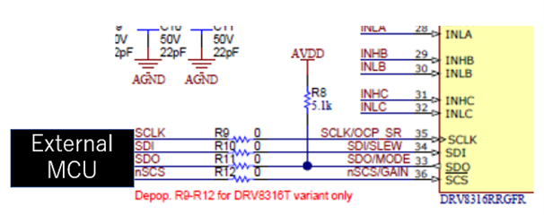
Our customer is evaluating DRV8316REVM by SPI communication of external MCU (don’t use TI MCU and GUI).

However, they can’t communicate to DRV8316REVM.


[Evaluation Status]

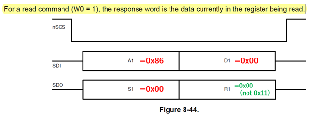
After reset, they read “Control__1 Register (Address = 0x3) [Reset = 0x11]”.

However, read value is 0x00 so they can't read the proper value and can’t write the proper value.


<Read Image>


We have two questions.


----------

[Q1]

When connected to external MCU(don’t use TI MCU and GUI),

-Is it necessary to change the setting of DRV8316REVM?

-Is it necessary to change the register or other setting?


-------


[Q2]

-When write command (W0 = 0), what value is output for " R1 of Figure 8-44"?

(For example, data of A1 address etc.)


-When read command (W0 = 1), What should I set for "D1 of Figure 8-44”?

(For example, any value is fine etc.)

----------


Regards,

Hide

  • Hi Hide,

    Thanks for posting to the MD forum! 

    When using external MCU with DRV8316REVM, ensure that the SPI initialization follows the SPI programming section of the datasheet (Section 8.5.1). Esnure that clock polarity and clock phase is set correctly so that data is captured on the falling edge of the SCLK pin and data is propagated on the rising edge of the SCLK
    pin, and the data is active high. 

    No hardware changes should be needed. 

    Thanks,

    Aaron

  • Hi Aaron-san,

    Thank you for your prompt reply.

    We would like to know about [Q2].

    I’d greatly appreciate your verification.

    Regards,

    Hide

  • Hi Hide-san,

    Regarding question 2, for a write command the value of output "R1" will be the contents of the register at address "A1" that is being overwritten. For example, if the contents of register 0x07 was 0x18, then if you write 0x24 to that register then you will see 0x18 as the value of "R1" during that SPI write. For a read command, the value set at "D1" doesn't matter as long as the parity bit is set such that the entire 16 bit command contains an even number of 1s. 

    If this answer as well as Aaron's answer are insufficient to solve the customer's issue, it would be helpful to have a waveform showing all 4 SPI signals on one plot during a SPI read command. This would allow us to compare the waveforms to the datasheet and see if we can find any issues. 

    Regards,

    Anthony

  • Hi Anthony-san,

    Thank you for the detail information and advice.

    Regards,

    Hide