This thread has been locked.

If you have a related question, please click the "Ask a related question" button in the top right corner. The newly created question will be automatically linked to this question.

DRV8353RS-EVM: Driver Output Signal Issue

Part Number: DRV8353RS-EVM
Other Parts Discussed in Thread: DRV8353,

Dear Team,

   As per the previous explanation on Motor Controller Unit, now we are moving in clear and strong way. So I expect to solve the below mention problem in DRV8353RS EVM.

   Now we are just trying to spin the motor using 6 step commutation (square wave generation) by start and stop control function of CHx and CHNx timer functions and not by duty control.

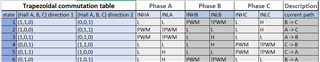
   We ensure the input to the gate drive is based on the Hall table and it is working perfect.

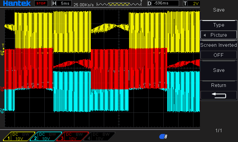
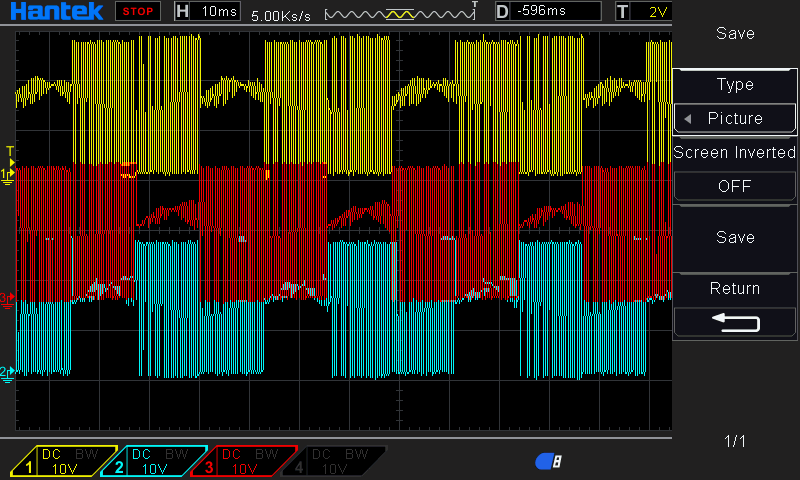
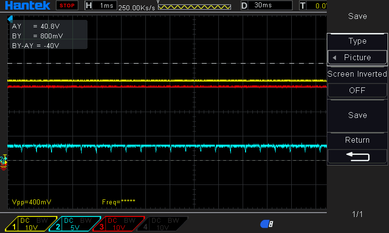
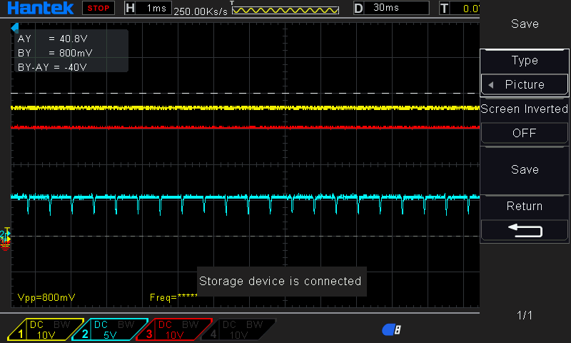
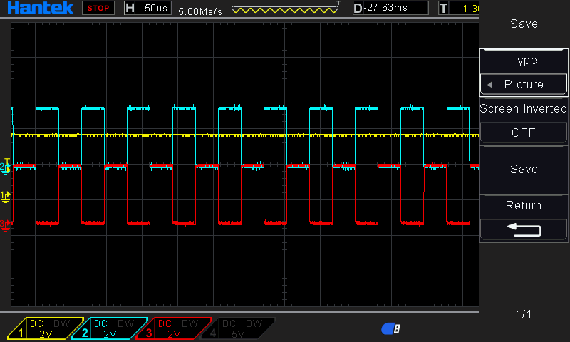
   While checking after gate driver all High side are getting enabled.

(for example Hall Position 001 : PHA-OFF, PHB-Negative, PHC-Positive; but actually after gate driver

GHA-ON(just an high state, no square pulse),

GLA-OFF,

GHB-ON (square Pulse),

GLB-ON (square Pulse),

GHC-ON (square Pulse),

GLC-OFF)

Expecting output of the above example is

GHA-OFF,

GLA-OFF,

GHB-OFF,

GLB-ON (square Pulse),

GHC-ON (square Pulse),

GLC-OFF


Kindly provide the solution fast, because we have very short time to complete the development.

Thanks,

Ramyaa R 

  • Hi Ramyaa R,

    Thanks for your question! I am assuming you are measuring from the high side gate to ground when you are taking these measurements. When a MOSFET is supposed to be off then the DRV will work to make sure that the gate to source of that particular MOSFET is 0V. So if the source voltage of the high side MOSFET increases and decreases, the gate voltage will do so as well to maintain 0V across the gate to source of the MOSFET. When one phase is pulsing on and off and another phase is in high z mode (meaning the MOSFETs of that phase are off), then the source voltage of the high side MOSFET of the phase in the HI-Z state will increase and decrease due to the coils of the motor acting as a resistor divider. I suspect that this could be what you are seeing. One way to confirm this is to use a differential probe and measure the gate to source voltage of the high side gates to make sure that they are not switching on and off. Another way to check would be to measure the high side source to ground and the high side gate to ground and see if they rise and fall at the same voltage.

    Regards,

    Anthony 

  • Dear Anthony,

    Thanks for your reply.

     I missed to add some points, but you found that by given inputs and awesome.

    I need to clarify some points on above method, we just using resistance load (star connection) instead of motor to avoid the nFault condition and over current conditions.

    While switching the MOSFETs the above mentioned steps are after gate driver (Gate driver output) and before the MOSFET input (pulse to the Gate)

    for reference please check the DRV 6 test points (GHx,GLx).

    The phase switching also changed (All the phase are getting enabled)

    Example :

    Hall Position 001 Expected: MOTA-OFF, MOTB-Negative, MOTC-Positive; Obtained : MOTA-ON (just high no pulse), MOTB-ON(Negative pulse), MOTC-ON(Positive pulse); 

    We just connect the motor in same condition and obtained the above mentioned state(example) and motor getting spin with noise at 350mA.

    Kindly provide the solution.

    Thanks & Regards,

    Ramyaa R

  • Hi Ramyaa,

    Thank you for your question! Would you be able to provide an oscilloscope plot showing the output of phases A, B, and C on the same scope plot? 

    What control mode are you using? are you using1xPWM mode? Or 6xPWM mode?

    Regards,

    Anthony 

  • Dear Anthony,

    Thank you for reply. 

    I have attached the Motor Phase voltage (while spinoff with noise).

    MOT_A = Yellow; MOT_B = Blue; MOT_C = Red;

    Please find the DRV8353RS EVM register configuration which we have set through SPI.

    DRV8353RS EVM Configuration

    Driver Control
      OCP_ACT[10]     0b = Associated half-bridge is shutdown in response to VDS_OCP and SEN_OCP        
      DIS_CPUV[9]     0b = VCP and VGLS undervoltage lockout fault is enabled        
       DIS_GDF[8]     0b = Gate drive fault is enabled        
      OTW_REP[7]     0b = OTW is not reported on nFAULT or the FAULT bit        
      PWM_MODE[6:5]     00b = 6x PWM Mode        
      PWM1_COM[4]     0b = 1x PWM mode uses synchronous rectification        
      PWM1_DIR[3]     PWM1_DIR = In 1x PWM mode this bit is ORed with the INHC (DIR) input        
      COAST[2]     COAST = Write a 1 to this bit to put all MOSFETs in the Hi-Z state        
      BRAKE[1]     Brake = Write a 1 to this bit to turn on all three low-side MOSFETs This bit is ORed with the INLC (BRAKE) input in 1x PWM mode        
       CLR_FLT[0]     CLR_FLT = Write a 1 to this bit to clear latched fault bits. This bit automatically resets after being writen        
    Gate drive HS
      LOCK[10:8]     011b to this register to unlock all registers        
      IDRIVEP_HS[7:4]     0011b = 150 mA        
      IDRIVEN_HS[3:0]     0011b = 300 mA        
    Gate Drive LS
      CBC[10]     1b = For VDS_OCP and SEN_OCP, the fault is cleared when a new PWM input is given or after tRETRY        
      TDRIVE[9:8]     11b = 4000-ns peak gate-current drive time        
      IDRIVEP_LS[7:4]     0011b = 150 mA        
      IDRIVEN_LS[3:0]     0011b = 300 mA        
    OCP Control
      TRETRY[10]     0b = VDS_OCP and SEN_OCP retry time is 8 ms        
      DEAD_TIME[9:8]     01b = 100-ns dead time        
      OCP_MODE[7:6]     01b = Overcurrent causes an automatic retrying fault        
      OCP_DEG[5:4]     10b = Overcurrent deglitch of 4 µs        
      VDS_LVL[3:0]     1101b = 1 V        
    CSA Control
      CSA_FET[10]     0b = Sense amplifier positive input is SPx        
       VREF_DIV[9]     1b = Sense amplifier reference voltage is VREF divided by 2        
      LS_REF[8]     0b = VDS_OCP for the low-side MOSFET is measured across SHx to SPx        
      CSA_GAIN[7:6]     10b = 20-V/V shunt amplifier gain        
      DIS_SEN[5]     0b =Sense overcurrent fault is enabled        
       CSA_CAL_A[4]     0b =Normal sense amplifier A operation        
      CSA_CAL_B[3]     0b =Normal sense amplifier B operation        
       CSA_CAL_C[2]     0b =Normal sense amplifier C operation        
      SEN_LVL[1:0]     11b = Sense OCP 1 V        
    Reserved
      Reserved[10:1]              
      CAL_MODE[0]     0b =Amplifier Calibration operates in manual mode        

    Consider the above mentioned board is working fine and in good condition and consider it as Board-B, another board which is in fault condition due to the low voltage of VGLS pin (below 4V) consider it as Board-A.

    We have tried to overcome the fault by reset condition of Enable pin, but still in fault condition.

    since we are working in curial situation, only one good board and another board in fault, so kindly help us by providing samples.  

    Thanks & Regards,

    Ramyaa R

  • Hi Ramyaa, 

    I will try to get back to you with a response by the end of the day today.

    Regards,

    Anthony

  • Hi Ramyaa,

    It would be helpful if I could see a zoomed in scope plot of phase A, B and C where only a few of the PWM periods are showing. This will give me more insight into whether or not the system is operating as expected. Is the waveform that you provided with a resistive load? Or is there a motor attached?

    Could you provide a waveform showing the INHx and INLx signals of 2 of the phases? For example, INHA, INLA, INHB, and INLB all plotted on the same oscilloscope plot. Could you provide a zoomed in version of these inputs to show the PWM frequency and duty cycle of the inputs? And then would you be able to provide a zoomed out plot of these same inputs? 

    The register settings you provided seems fine. 

    I am not sure if you are needing more EVMs or just the drivers, but you can order more EVMs here under the "Order & start development" section or you can order the driver itself here

    Regards,

    Anthony 

  • Dear Anthony,

    Thank your reply.

    We have two DRV8353RS-EVM and we spinout the motor successfully and tried to capture the 6 PWM signals, but both the boards are in same nFault condition due to VGLS pin under voltage condition. As per the pervious mentioned driver setting we spinout the motor and we tried to recovery the fault as per the DRV8353 datasheet (Reset of Enable pin, CLR_FLT bit was in zero). And now we don't have any working board, we need to complete it by next month end, so kindly advice to solve these problem without changing the Driver IC and if you could able to arrange the DRV8353RS IC sample, please do the needful.

    Thanks & Regards,

    Ramyaa R

  • Hi Ramyaa,

    I would recommend ordering more EVMs directly from the DRV8353RS-EVM webpage since these will immediately ship. You can also order the DRV8352RS IC here.

    When did the faults first occur? What happened leading up to the fault? Did the fault first occur when the motor was attached? or when you were using the resistive load (star connection)?

    Can you provide a scope plot showing the VDRAIN voltage, the VGLS voltage, and the VCP voltage of the driver? Could you do this same test for both boards when the boards are powered up?

    Prior to the issue with the under voltage fault, were you able to capture a zoomed in scope plot of the outputs of phase A, B, and C showing a few of the PWM waveforms? This would help me analyze the duty cycle that is present at all these 3 phases. Also, for the scope plot that you provided earlier, was that captured when using a resistive load attached to the phases? Or was the motor attached?

    You may consider reducing the IDRIVE to the lowest setting (50mA/100mA) since the Qgd of the MOSFETs on our EVMs are really small, and depending on what motor you are using and how you are driving your motor the 150mA/300mA setting may still be too high. If the IDRIVE you are using is too high for your particular application then this can damage the driver and sometimes can result in damaging the VGLS regulator.

    It would be good to check to make sure that the SPI has finished writing to the registers prior to starting your PWM commands. This is important since if you try to drive the motor before the IDRIVE setting in SPI has been configured to the desired setting then that could cause damage to the driver. 

    Regards,

    Anthony

  • Dear Anthony,

    Thanks for your response.

    First point the above attached phase characteristics is taken while motor getting spin and now we can't zoom the plot because it was in image format and we can't able to take the new plot also, because both the driver boards are in fault condition.

    All these development and output mentioned to you is our own code with own microcontroller (using 6 step commutation, just a PWM switching done based on the hall input to run the motor at constant time period without any fault and just fault condition based enable pin toggle is done). Before these we have already checked your TI based Insta spin FOC in Launch ISO-F28027F with DRV8353RS (both the boards) and it was spinout successfully and speed varied using DRV8353RS GUI  for long time with same Driver SPI register setting(without any fault condition). These TI based Motor spinout implemented with the motor and the same motor currently we are using. 

    We are also confirmed the SPI response from the device for each time and we just printing the SPI response in UART for cross verification of the respective transmitted address. 

    In own code, we just doing the basic timer overflow interrupt to read the Hall position and based on the Hall position just switching the PWM (ON and OFF with constant duty) and for fault condition identification, just reading the nFault pin and if fault occurs the enable pin will be toggled.

    I have attached the VGLS, VCP, VDRAIN voltage characteristics (YELLOW - VCP, BLUE- VGLS, RED- VDRAIN) for both the boards.

    Board B

    Board A


    Thanks & Regards,

    Ramyaa R

  • Hi Ramyaa,

    Thank you for your reply! I will try to respond tomorrow.

    Regards,

    Anthony 

  • Hi Ramyaa,

    After taking a more in depth look at the waveforms you provided of your commutation sequence, it looks like the method of commutation that your controller is using is a little different than the typical trapezoidal method that is normally used, and I believe that could be causing some adverse effects which could damage the motor driver. When you are able to order a new EVM I would recommend checking the outputs of your controller (going to the INHx and INLx pins) to make sure that they are outputting the appropriate signals based on the table below:

    Where PWM is a PWM waveform with a particular duty cycle to turn on and off the corresponding FET with that PWM, and PWM! is the inverse waveform of the PWM waveform. for instance, if the PWM signal was high for 70% and then went low for 30% of the period, then PWM! would be low for 70% and then go high for the remaining 30% of the period. 

    If the outputs of your microcontroller are not corresponding to this table then you may consider adjusting the code of the microcontroller to achieve the outputs based on the table. If you still have problems after that please let us know and would be happy to look into the issue further.

    Regards,

    Anthony 

  • Dear 

    Thanks for your reply.

    As you mentioned, the trapezoidal commutation table based on the hall input; just we modified the code. Based on your table format the Microcontroller output has been obtained, due to nfault condition we cant able to check in DRV8353RS EVM board and we have ordered the new DRV8353RS IC, once it received we will check it.

    Now, we have attached the image for one of the step in the table,

    HALL position (Hardcoded) : 001 - GLB : High, GHC : PWM, GLC : !PWM (Other channel are Low)

    GLB - Yellow, GHC - Blue, GLC - Red

    Thanks & Regards,

    Ramyaa R

  • Hi Ramyaa,

    As long as the other input pins are low, these input waveforms look correct. When I compare these input signals here to the phase signals you provided earlier, the phase signals are not showing the correct operations if the above plot was the input. Since GLB is high, that means that the low side MOSFET of phase B would continually be on and pull phase B to GND while at the same time we would see a PWM waveform on  phase C. But we can see in the phase output plot below that phase B is actually showing a PWM response (blue trace) instead of being constantly held to GND. 


    Once you get a new EVM it would be good to probe the INx pins again during the operation of the motor just to make sure that during motor operation (without hardcoding any parameters) there isn't any difference between the expected signals and the actual signals (based on the table I provided). If all the inputs are behaving as expected, then could you provide waveforms by using a differential probe on the gate to source signals of the high side and low side MOSFETs to make sure they are turning on and off as expected based on the input pin commands? If you don't have differential probes you can just measure the gate to ground voltage instead of the gate to source (just keep in mind that the gate to source voltage is what determines if the MOSFET is on or off, as opposed to the gate to ground). 

    Regards,

    Anthony,

  • Dear Anthony,

    Thanks for your clarification.

    Please don't get confused with Motor Phase image(April 23rd) and it was based on six step commutation(Just passing PWM to respective Hall based input).

    But yesterday's image was take only at Microcontroller's output(Based on your Trapezoidal commutation logic) and we doesn't connect with Driver and motor, so we doesn't upload any motor phase image. Only after receiving the new IC, we could be able to check the suggested Trapezoidal logic, yesterday's image was only just the output from microcontroller.

    Thanks,

    Ramyaa R

  • Hi Ramyaa,

    Thanks for the explanation. Looking forward to reviewing the data from the new IC when it arrives.

    Regards,

    Anthony 

  • Hi Ramyaa,

    It has been a while since we heard from you last, have you received the new part yet?

    Thanks,

    Matt

  • Hi Ramyaa,

    I am going to close this thread for now. If you have further questions, please click the "Ask a related question" button at the top right of the screen.

    Thanks,

    Matt