This thread has been locked.

If you have a related question, please click the "Ask a related question" button in the top right corner. The newly created question will be automatically linked to this question.

TPS543B20: TPS543B20 for stable operation at 2MHz

Part Number: TPS543B20

Hi

I want to know about the following
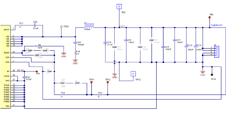
Vin: 12V
Vout: 0.9V
Iout: 25A
L: EVM Default@0.47uH
Cin / Cout: EVM Default

RAMP = 187K , CRAMP = 14.1pF (Default)

Fsw: 450KHz ⇒ When operating at 2MHz

Is it correct to recognize that it is necessary to change the resistance value (= Cramp) of RAMP in order to obtain the generally recommended phase margin: 45deg and gain margin: 10dB?

If Yes, how can the formula / method be used to calculate the appropriate RAMP resistance value?

Also, please tell me any other precautions for operating at 2MHz.

Thanks

Suzuki

  • Hi Suzuki,

    As far as operation at 2MHz goes, it is important to be aware of the on-time limits. For the PVIN=12V and Vout=0.9V configuration, you would have enough on-time margin for this part. If PVIN is expected to go much higher, then the on-time boundary may need to be considered.

    For the Ramp compensation, increasing the ramp resistance in general leads to a higher gain, higher crossover frequency, and lower gain margin. However, the phase margin is not a direct function of the ramp resistance and depends on output capacitance, inductance, and switching frequency. Therefore, it is normal to have to adjust the ramp resistance when modifying a design parameter such as switching frequency. There is not a well developed formula for optimizing the ramp resistance value. However, I could share a device calculator or set of tables that can help you make a better determination regarding the ramp resistor and its effect on phase margin and gain margin.

    Regards,

    Alec Biesterfeld

  • Hi Alec san

    I want to check the frequency characteristics using FRA (Frequency Response Analyzer). Is TPS543B20E possible?
    If possible, as you know, the FRA should inject the signal at the OSC.Normally, a signal is injected between the output and the FB resistor. Where should I inject ? 

    >> I could share a device calculator or set of tables that can help you make a better determination regarding the ramp resistor and its effect on >>phase margin and gain margin.

    ⇒Can you share the above information with me? It would be nice to know the correlation between the Rramp set resistance and the phase / gain margin.
    The condition is Vin = 5V Vout = 1V Iout = 25A

    Thanks

    Kotaro Suzuki

  • Hi Suzuki,

    On the schematic you shared, I would recommend changing the R13 to a 10-50ohm resistor and injecting an AC frequency sweep at TP11 and TP12.

    Please email me at a-biesterfeld@ti.com, and I can share the information regarding the phase/gain margin calculation in further detail.

    Regards,

    Alec Biesterfeld