This thread has been locked.

If you have a related question, please click the "Ask a related question" button in the top right corner. The newly created question will be automatically linked to this question.

TPS53015: FET Selection ( Half Bridge vs Discrete)

Part Number: TPS53015
Other Parts Discussed in Thread: CSD17507Q5A, CSD86336Q3D, CSD86350Q5D, CSD87351Q5D

Hi,

We are planning to use TPS53015 part in our board. Our system requirements are listed below.

1. 19V input (+/-5%), 3.3V Output
Output Current : 7A
Operating Temperature : 0C to 50C

2. 19V input (+/-5%), 5V Output
Output Current : 6.5A
Operating Temperature : 0C to 50C


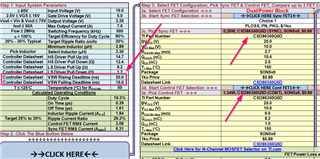
The application design in TPS53015 datasheet uses discrete FET CSD17507Q5A parts. With the help of TI's FET loss calculation sheet, We were able to calculate the FET losses to determine the maximum ambient temperature with & without external gate resistor(for HS FET only). We have tabulated the values in the attached sheet (refer "FET Loss (Discrete)" sheet). We have also considered half bridge FET parts (CSD86336Q3D,CSD86350Q5D) based on the FET loss calculation sheet and tabulated the loss and max ambient temperature values in the sheet (refer "FET Loss (Dual)" sheet).

Based on the CSD17507Q5A datasheet, the Rja values are dependent on copper area connecting the DRAIN pad. Datasheet suggest that for minimum DRAIN pad area, Rja would be 125C/W. Although, it may be possible to have greater copper area for VIN trace connecting the DRAIN of the control FET, the copper area connecting the DRAIN of sync FET needs to be minimal as per our understanding as its SW node.
Q1) Under this condition, We wont be able to meet our product's ambient temperature requirement of 50C. Could you please let us know is there a way to overcome this to use discrete FET?

The dual FET parts identified from FET loss sheet appears to have PGND pad which can be used connected to GND for heat to escape from FET. Our design would have atleast 2 GND planes and we think this should help lower the Rja value.
Q2) Could you please let us know if its fine for us to use any one of the suggested dual FET part with TPS53015 (0C to 50C) ?

The FET loss value has increased atleast by ~0.3W with inclusion of 10Ohm gate resistor to HS FET. The application design includes that same only HS FET not for LS FET. The additional loss brings down the calculated max ambient temperature closer to 50C. (Note: 10 ohms was added on top of the max HS Driver pull up/pull down values of TPS53015 to calculate loss)
Q3) Is it fine to replace the gate resistor with zero ohms? Also, Do we need include one for gate of the LS FET as well?

We have also attached TI's FET sheet which we had used for loss computation. Let us know if you find anything off with the values.

We will look forward for your reply at the earliest as we are in the middle of the design.

Thanks,
Balaji

TPS53015.zip

  • Hi Balaji,

    Thanks for your detailed information. Peter is looking into this and will feedback to you soon.

    Thanks,

    Lishuang

  •  

    1) Yes, Clip-Stack Dual MOSFET configuration, which provides a large ground pad connected to the source of the Synchronous Rectifier is intended to provide an easier way to connect the power-dissipating FETs to a thermal plane of effective heat spreading and reduced Junction to Ambient thermal resistance.  Where a discrete FET solution needs to connect the largest heat-dissipating device in the circuit - the low-side Synchronous FET to the node that must be kept the smallest for EMI reasons - the switching or phase node, The co-packaged dual FETs allow easy, direct thermal connection to the largest thermal area on a typical PBC - the ground plane.

    Providing direct thermal via connections from the integrated thermal pad to 2 layers of ground PCB can significantly lower the thermal resistance to ambient air.  Thermal resistance of 30°C/W and less have been achieved when combined with top and bottom layer ground area and the ground planes are not blocked or cut by excessive via passthroughs.

    2) Series Gate Drive resistors are commonly added in series with the gates of Power MOSFETS for several reasons. 

    1. Reduce inductive ringing of the gate-drive voltage, which can induce an over-voltage condition on the gate and potentially damage it. 
    2. Reduce switching node overshoot and ringing due to the fast turn-on of the control FET
    3. Control high-frequency content of the rising and falling edge of the switching node.

    In order to obtain some of these benefits with less power dissipation, I would recommend selecting resistors smaller than 10Ω.  I would also recommend splitting the resistor into 2 parts.  One resistor between the SW pin and the source of the control FET will limit the turn-off slew-rate when HDRV pin is internally pulled to SW, and a second resistor in series with the VBST pin to control the slew-rate of the turn-on.  As long as the VBST to SW capacitor is connected on the MOSFET side of the SW series resistor, the resistor will not affect the turn-on rate.  These two separate resistors will allow the rising and falling slew-rates to be tuned to provide the best efficiency while still limiting the EMI and FET voltage stress associated with the high-side Switching.

    With good bypassing of the drain of the control FET to the source of the synchronous FET, and low impedance source in the 50-200MHz region, it is typically possible to design a power converter that does not require any resistance and can operate with 0-Ω, but it is also generally recommended as good design practice to provide provisions for these resistors in the event that the layout produces more parasitic inductance and ringing than is acceptable.

    A good practice provides a very small (0201 or 0402) 2.2-10nF capacitor very close to, or directly underneath the Drain to Source of the high-side FET to minimize the source impedance in this critical 50-200MHz range.

    Because the LDRV voltage is sensed as part of the adaptive dead-time control circuitry, adding a resistor in series with the LDRV pin is not recommended and could lead to pre-mature turn-on of the control FET and cross-conduction.

  • Dear Peter,

    Thanks for the detailed reply!

    1) According to my understanding of your reply, Dual MOSFET configuration is the way to go to have both minimal Switching node area and improve thermal conductivity with GND vias.

    Regarding which FET to go for among the two CSD86336Q3D & CSD86350Q5D parts. CSD86350Q5D looks to be good option from thermal standpoint despite being slightly more lossy than CSD86336Q3D.

    However, the rise/fall time values of the CSD86350Q5D FET seems seems to be on the higher side when compared to the dead time values of TPS53015 chip (15 to 20ns). Should I be concerned about the cross-conduction here? If CSD86350Q5D is a no-go, then CSD86336Q3D would be fine?

    I am asking this because I am so far under impression that TI FET Loss sheet takes care of compatibility with driver IC as I input the dead time values from the TPS53015 datasheet.

    Kindly let us know on this. Also, let us know your suggestion on what would be best pick among these two (or others if any).

    New Question
    2) Is there a possibility for input voltage to reach the output (via HS FET) when input voltage is rising? During this condition, driver chip may not be powered up to drive the gates causing HS FET gate to float and turn on.

    Thanks,
    Balaji

  •  

    1) Yes, TI's packaging of the Dual FETs generally provides for a smaller size foot print while providing for good thermal power dissipation.

    2) I would not be concerned with cross-condition regarding the turn-on and turn-off time listed in the CSD86350Q5D MOSFET, the adaptive dead-time control of the TPS53015 will ensure the complimentary FET is turned off before allowing the other FET to turn-on as along as there is no external resistance added to the LDRV pin path to the gate.

    My one concern using the CSD86350Q5D in a 19-V input application is the possibility of excessive ringing on the switching node resulting in over-voltage on the 25V rated power-FETs.  You'll need to pay very close attention to layout and bypassing to ensure the switch node does not ring to high during the turn-on of the control FET and the Drain to source voltage on the control FET does not exceed 25V during the control FET turn off when parasitic inductance drive the drain up at the same time the source if dropping below ground.

    3) The TPS53015 drivers include weak passive pull-downs to hold the FETs gates off during dV/dt rise of VIN even if the TPS53015 is not powered.  However, if the input voltage is expected to rise faster than 10V/ms, you may want to consider a 1k to 10k resistor from HDRV to SW and/or LDRV to GND to provide additional gate discharge capability.

  • Dear Peter,

    Thanks for your reply!

    I understood your point on the voltage rating and ringing in SW node. I was able to pick 30V abs max (27V recommended) rated part CSD87351Q5D which looks to be suitable.  Kindly let me know if you have any comments or concerns on the same.

    As per your suggestion, We will consider an optional 10k PD between HDRV and SW for HS FET to prevent inadvertent output voltage. For LS FET, OCL programming resistor would do the job.

  •  

    The CSD87351Q5D should be a very good option with more voltage stress margin for your application.