This thread has been locked.
If you have a related question, please click the "Ask a related question" button in the top right corner. The newly created question will be automatically linked to this question.
Hi,
I'm using this part as a buck boost where my input voltage is 10V to 30V and my output is 18V, 6A. My schematics are below:
My input is 12V from a benchtop power supply and is very clean. This is eventually going to drive additional power supplies and eventually a comExpress module. When I used the comexpress module, the 18V dips down to 6.2V when the comexpress starts to boot and draw current and then my system resets and goes into this continuous hiccough mode.
To simplify debug, I took off the comExpress module and simply put a constant current electronic load on the supply. With very little load on the supply, I scope the boost SW2 signal and it is switching at the appropriate frequency. SW1, the buck side is not switching. Everything seems normal.
When I begin to increase the load current to about 1.6A, then device begins to fall out of regulation as shown:
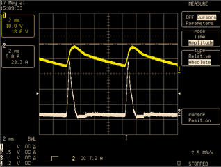
The yellow trace is the 18V output which beings to dip and the white trace is the input current and goes to almost 18A!
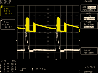
Below is the Boost SW2 node.
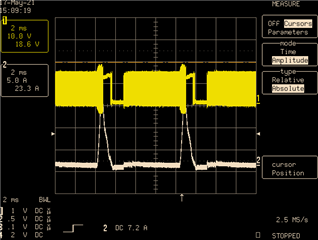
And below is SW1 which is the buck node.
If I slowly reduce the electronic load, everything begins to work well again. Thinking that maybe the ILIM resistor was populated with an incorrect value, I removed it from the board and measured it. It was 20K. I tried a 10K but the behavior is the same.
I have also tried the follow:
* removed R9 which basically pulls up the UVLO to the 12V input.
* I was able to sneak in a 24.9K from MODE pin to ground and that did nothing.
All the values were gotten from Power designed. The inductor is rated for 25A and has a DCR of 5.11mOhm so this should be more than enough for this system.
The layout followed the datasheet recommendations so I'm pretty confident that it is good.
Why is this device behaving so poorly?
Thanks!
John
Hi John,
Thank you for reaching out.
Per your description that the device works normally at light load condition but is abnormal at heavy load, it would be great if you can share your layout with us to double check.
Besides that, I want to remind you that TPS552882 thermal rise would be really high in the condition of Vin 10V, Vout 18V/6A because this IC integrates two Boost-side MOSFETs. In the minimum Vin scenario, the device is working in Boost mode so main switching loss, conduction loss is inside IC. Will you want to output 18V/6A from 10Vin?
Hi Zack,
Below is a snippet of the layout. It is very close to the example in the datasheet.
The system operates off either a 3 cell Lithium battery back or car battery. Battery is 10V to 30V which battery pack is 10.5V to 12.6V. Nominal for the battery pack is 11.1V and for the car battery 12V. Although we can run with a low battery at 10.5V we typically will be about 11V worst case.
Thanks,
John
Hi John,
The layout looks pretty good. Only little needs to be improved:
1. Add 3~4 GND vias close to VCC cap GND pad.
2. To minimize gate-loop area, High side FET gate and source traces are routed side by side as differential pairs.
3. It would be better to add one 1uF or 0.1uF low ESR 0603/0402 package ceramic capacitor close to IC Vout pin and GND pin.
4. Add a 1uF or 0.1uF decoupling capacitor close to VIN pin.
The above layout comments are just suggestions but I don't believe it will cause this issue.
To debug the issue, please help provide:
1. Have you set the benchtop power supply current limit high enough? What's the current limit value you are setting now?
2. Could you also probe Vin waveform? Also check VCC pin waveform.