A related question is a question created from another question. When the related question is created, it will be automatically linked to the original question.
If you have a related question, please click the "Ask a related question" button in the top right corner. The newly created question will be automatically linked to this question.
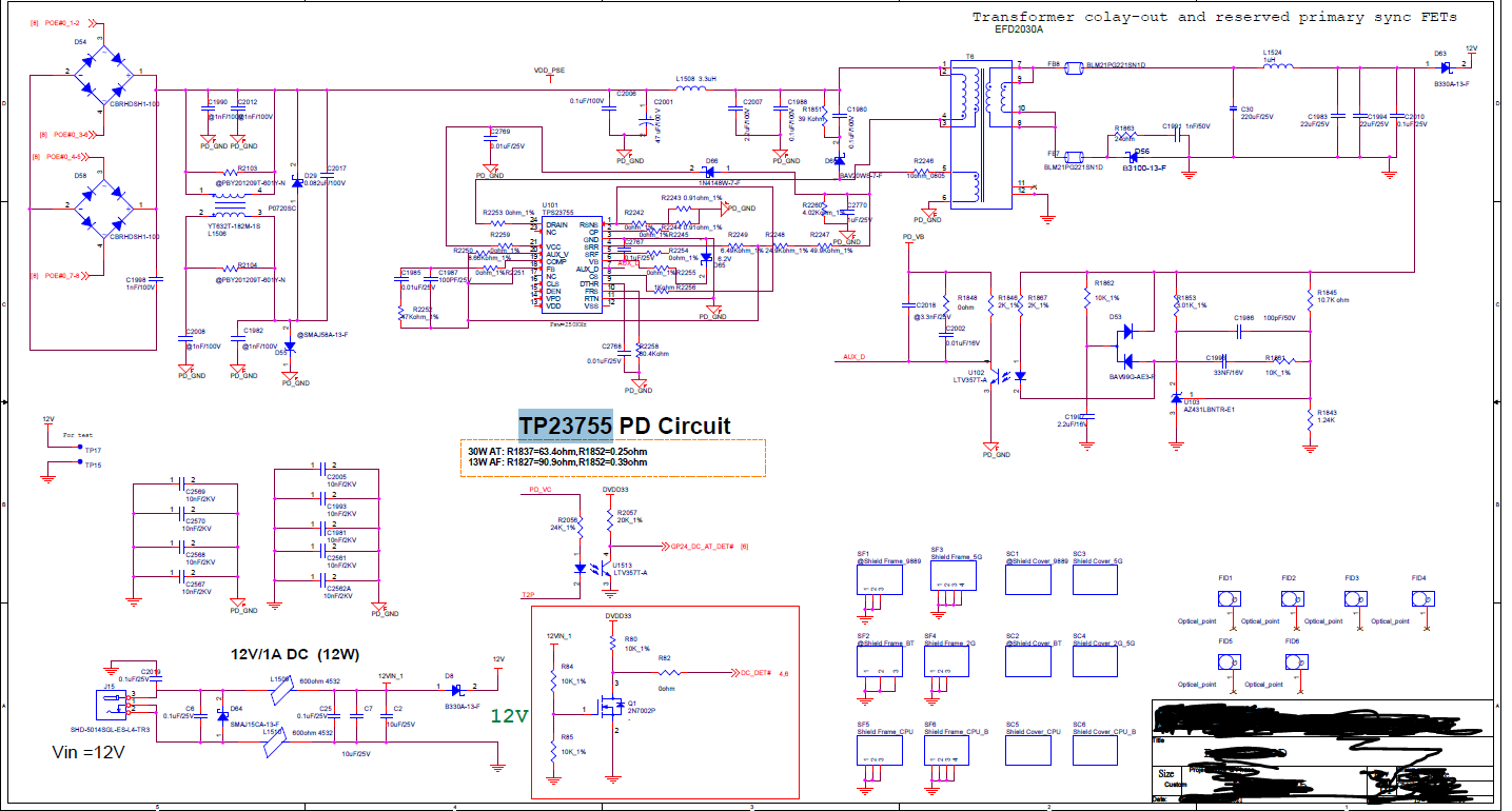
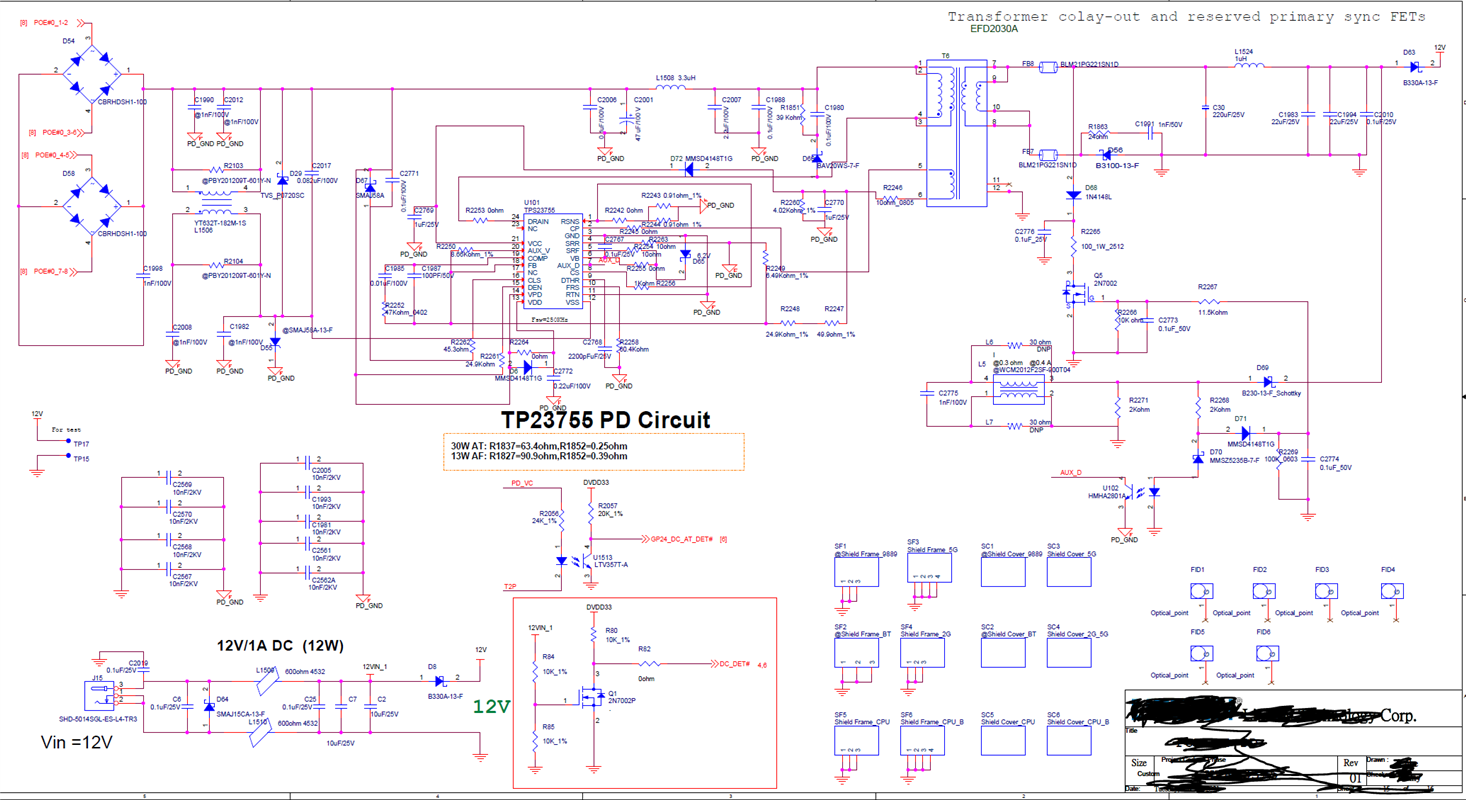
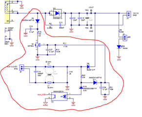
I have some concerns about this design as it currently is.
The transformer dot convention is incorrect.
I also don't recommend the ferrite beads on the secondary.
I also don't recommend the power diode on the low side, I recommend on the high side of the output.
All in all, I am worried about the design, and I recommend they copy the TPS2755EVM-894 as this is known working solution for 12V.
Also of note is that the AUX_D opto feedback circuitry is not required for designs that do not require adapter priority. It looks like they are diode ORing the 12V adapter on the output directly, and if that is the case, the opto feedback components can all be removed.
Let me know if you have any question about this. Thank you.
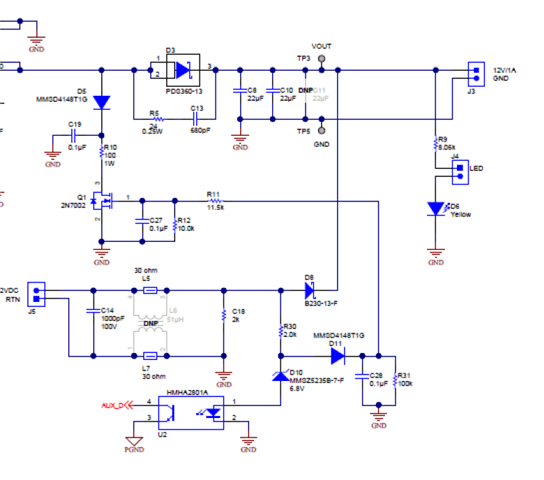
The circuitry circled below enables the adapter to have priority over PoE:
In the customer schematic, they can add the 12V adapter input across C2775, similar to the TPS23755EVM-894 schematic shown above. This will enable the adapter to have priority over PoE.
Alternatively, a more simplistic way to enable adapter priority is to diode OR the 12V adapter on the output. For the adapter to have priority, they would need to make sure the PoE output voltage is always lower than the minimum voltage of the adapter.
Please also see my feedback below based on the schematic:
For D29, you can keep this on the board, but this may impact the detection current because the off-state leakage current is 5uA. May end up needing to DNP.
Recommend to change C2017 to 1nF.
Must connect the node located at the anode of D67 to VSS.
I assume what is labeled GND1, GND2, GND3, AND GND4 are the A1, A2, A3, A4 Anchor pins on the TPS23755. These are all connected to PGND but that is not correct. I recommend:
A1 needs to be connected to RSNS.
A2 needs to be connected to VSS.
A3 needs to be connected to VDD.
A4 needs to be connected to DRAIN.
I assume what is labeled GND5 is the PAD. If so, I recommend this be connected to VSS.
The VPD/VDD pin connections are incorrect. For instance, D6 can be removed and C2272 can also be removed. R2264 should be connected to VSS. Please reference TPS23755EVM-894 for how to connect these pins and the components.
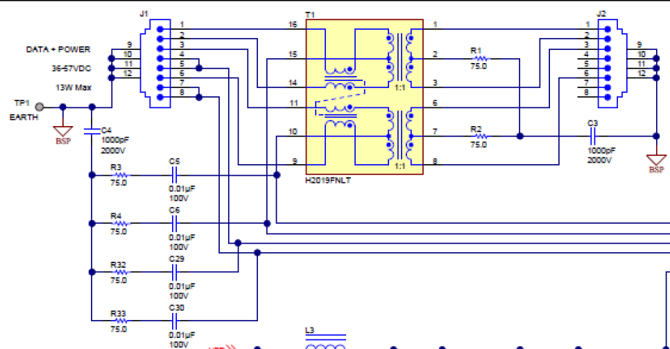
Recommend to add 2kV caps to secondary ground from pin 2 of transformer as shown in TPS23755EVM-894.
Recommend to not use BAV20WS-7-F for D68 and to instead use similar diode as in the TPS23755EVM-894 (voltage rating, current, and reverse recovery time) otherwise it could damage the FET.
Recommend to use 680 pF for C1991.
I recommend to add a 0ohm resistor in parallel with the output inductor L1524 as this may help with regulation. The inductor may make the regulation worse.
Recommend to remove D63.
Also of note is that the IC pinout isn't correct, recommend to correct this.
Let me know once these changes are made and I can do another review. Thanks!
The application don’t use the adapter. So remote AUX_D opto feedback circuitry. For 10mA MPS, they maintain R2265 as dummy load. I follow up your recommend and the customer modified the schematic(mark green cycle). Could you help to review the schematic?
For D29, you can keep this on the board, but this may impact the detection current because the off-state leakage current is 5uA. May end up needing to DNP. - Change to NC Recommend to change C2017 to 1nF. - modified Must connect the node located at the anode of D67 to VSS. - modified I assume what is labeled GND1, GND2, GND3, AND GND4 are the A1, A2, A3, A4 Anchor pins on the TPS23755. These are all connected to PGND but that is not correct. I recommend: A1 needs to be connected to RSNS. A2 needs to be connected to VSS. A3 needs to be connected to VDD. A4 needs to be connected to DRAIN. I assume what is labeled GND5 is the PAD. If so, I recommend this be connected to VSS. - modified The VPD/VDD pin connections are incorrect. For instance, D6 can be removed and C2272 can also be removed. R2264 should be connected to VSS. Please reference TPS23755EVM-894 for how to connect these pins and the components. - modified Recommend to add 2kV caps to secondary ground from pin 2 of transformer as shown in TPS23755EVM-894. - modified Recommend to not use BAV20WS-7-F for D60 and to instead use similar diode as in the TPS23755EVM-894 (voltage rating, current, and reverse recovery time) otherwise it could damage the FET. - modified Recommend to use 680 pF for C1991. - modified I recommend to add a 0ohm resistor in parallel with the output inductor L1524 as this may help with regulation. The inductor may make the regulation worse. - modified Recommend to remove D63. Also of note is that the IC pinout isn't correct, recommend to correct this. - modified
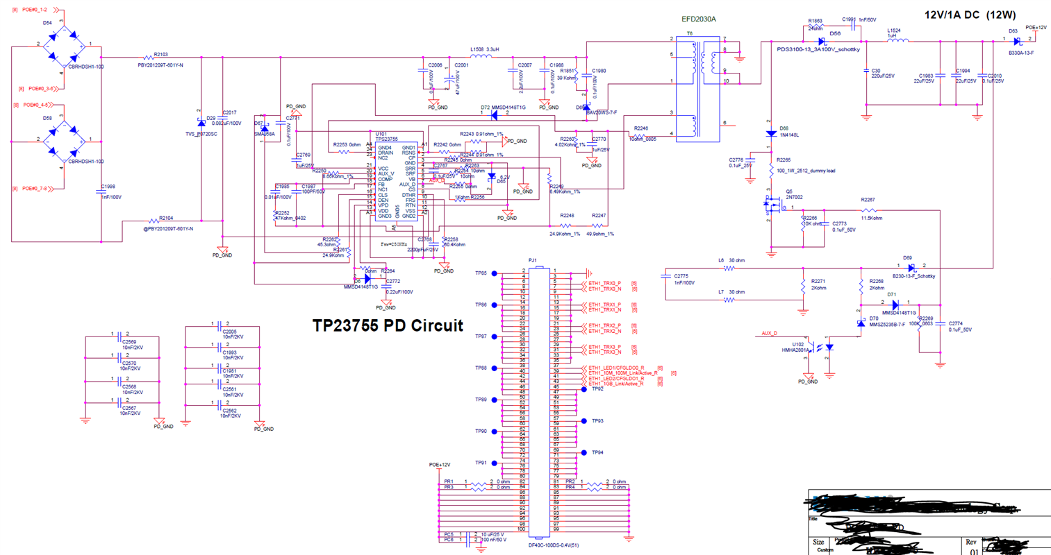
I recommend to change the resistor dummy load to 0.5W (285 ohm and rated for 1W) so as to not dissipate too much power and I also recommend this resistor be moved to the right of the output inductor.
Of note is that majority of customers real application load is able to supply the 10mA required MPS current without the need for a dummy load. I'm not sure the dummy load will be needed in the end but customer can always DNP the dummy load if they can meet MPS with their real load.
1. In the schematic you posted, VPD and VDD are connected with a 0 ohm resistor, so electrically they are the same node.
2. Yes that is what these pins connect to. Think about the primary power path, this is the positive side of the primary power.
Additionally, we would greatly appreciate it if you could please post new questions in new threads. This helps us keep track of questions and answers, and know if a schematic question got resolved, while a layout question is being answered. Thank you.
If this post answers your question, please indicate so by marking this thread as resolved. Thank you.
Thanks your recommend, the customer have some concern about changing package size of capacitor.
Could you help to recommend?
Because the size of PCB board will reduce, Therefore, C1980/C2770/C2771 require miniaturization.
Package of capacitor will changed from 0805 to 0603, but the capacitance and voltage specifications (100nf/100V and 1uF/25V) are the same, and both are X7R.
Will the package of capacitor change to be other risks?
Reducing C2770 to 06003 but keeping the voltage rating typically drives up cost, correct? Either way, to check if it is acceptable operationally is to confirm startup. VCC is the input power for the IC, and the capacitor C2770 provides energy for the startup operation. So customer needs to check full input voltage range and full load range to ensure there is enough effective capacitance on the board.
For C1980, my concern is the effective capacitance rating affecting the performance of the capacitor. This capacitor is part of the RCD snubber that is protecting the integrated switching MOSFET (between DRAIN and RSNS). The voltage cannot exceed 150V. The customer can check the VDS leading edge transient to ensure the reduced capacitor size is effective. Ensure the customer removes any filtering on the oscilloscope in order to see the true highest voltage across the FET.
Denny, you have asked multiple great questions. As TI transitions to BU support on E2E, I would love if other engineers could search these questions and answers. It helps future engineers and the BU if each set of questions is a separate post, so that the questions are searchable. I understand these questions are all for the same project, but please understand your questions could apply to many projects.
For future questions on this project, please create a new post. Thank you for understanding Denny.
If this post answers your question, please indicate so by marking this thread as resolved. Thank you.