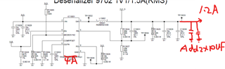
The capacitance Cff of this Feedback, How is it calculated?
This thread has been locked.
If you have a related question, please click the "Ask a related question" button in the top right corner. The newly created question will be automatically linked to this question.
Hello user,
Cff value was calculated during development. In Table 10-2 of the datasheet, you can find a recommended setting for the resistive divider and Cff values according to the output voltage regulation required in your Application.
Do you have any specific concern here ?
Let us know.
Thanks a lot!
Regards,
Dorian
I know the recommended capacitance value, but when I use this IC at present, I found that if the capacitance is changed to 68pF, the waveform duty cycle of the switch port is unstable, so I want to know the specific calculation method of the capacitance value.
Hello,
The selection table recommends settings that we used during validation and provides fast and stable responses.
May I know why are you willing to change the Cff value to 68pF ? What is the VIN/VOUT condition for which you are using TPS62810-Q1 ?
Let us know.
Thanks a lot!
Regards,
Dorian
We are using TPS62810-Q1 (4A), at the current DV stage, Vin=3.3V, Vout=1.1V, Iout=1.2A, 68pF is used, because the positive margin of output voltage is better, but the SW port waveform duty cycle Unstable.
Hello,
Could you share with us SW waveform where you observe this duty cycle instability ? Does it happen only at 1.2A output load ?
Was it a phenomenon you also observed with a 10pF Cff ?
Let us know.
Thanks a lot!
Regards,
Dorian
This is the waveform when Cff is 68pF, and the output capacitance is 50uF. When there is no load, the duty cycle of the SW port is already unstable. When the output electronic load is 1.2A, the waveform of the SW port is also unstable.
When the Cff is changed to 10pF, the duty cycle waveform of the SW port is very stable, but as mentioned above, the positive margin of output voltage is not better at this time, so can you provide the calculation formula for Cff?
Hi Meng,
I am taking over this topic while Dorian is out.
Have you tested with just a resistive load? It is very common that electronic loads and their control loops interfere with the IC and create bad waveforms.
On the Cff, we recommend just using a 10pF cap. There is no calculation to do.
Can you share the data you have that shows the 'positive margin of the output voltage'? I don't know what this means.
Thanks,
Chris
But when there is no load, the waveform of the SW port is also like this, which is unstable.
Ah, sorry that I missed that note.
Are you testing on the EVM or your own PCB? Can you share the schematic?
Chris
Thank you for sharing the schematic. It looks ok, though you may be on the edge with just 40uF nominal output capacitance. Can you share the part number used for those 10uF caps?
I would suggest adding 1 more 10uF Cout and seeing if this fixes the SW node waveform.
Can you share the measurements with the 10pF Cff? I'm still unclear what was the issue with this cap value.
Thanks,
Chris
The part number of those 10uF caps is "GCM21BR70J106KE22*, Murata";
We have adding 1 more 10uF Cout, but the waveform of the SW port is also unstable. Because when there is no load, the waveform of the SW port is also like this, which is unstable.
If changed the Cff to 10pF, the waveform of the SW port is very stable.
The waveform of Cff (68pF)
The waveform of Cff (10pF)
but as mentioned above, the positive margin of output voltage is not better at this time.
Thank you for trying the extra output cap.
I do not understand what you mean by 'positive margin of output voltage'. Can you explain this in more detail and/or show a measurement?
Chris
Ah, ok. Thank you for explaining.
Your circuit here looks very different from the circuit in that ppt slide: both FB resistors are different, the inductance is different, and the output cap is different. That slide should not be read as a general statement that a 68pF Cff is better than a 10pF one. Which Cff value is best entirely depends on the exact circuit being tested.
As well, are you testing on the EVM or on your own PCB? A non-ideal layout can couple in noise, where you might see this sort of SW issue.
Chris
Hello Meng,
Do you have any updates on Chris's questions above ?
Let us know if you have any further questions.
Thanks a lot!
Regards,
Dorian