Lm5010 works as 15V converter for MOSFET drivers, Vin 48V. LM5010 is followed by the Efuse TPS6623 working as protector, just in case LM dies and 48V input voltage propagates to rest of the system. The 15V is used to make 5 and 3V3, which inputs are not 48V tolerant; this is why efuse is used.
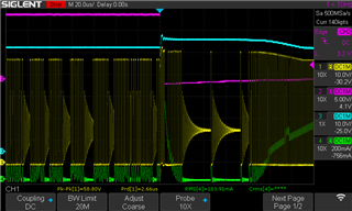
I enclose schematic and wave plots. Situation is as following: system starts Fig.1, we see nice soft-start, after 50ms 3 mosfet drivers get low signal from uC which starts to charge their relative big bootstrap caps 4u7, x3 pcs.( not in circuit visible)
This makes for sure current surge, 6 fets have 15 Ohm gate resistor. Theoretically this should limit surge current to 1A. They are not start simultaneously its is 3ph Hbridge.
What I do not understand is:
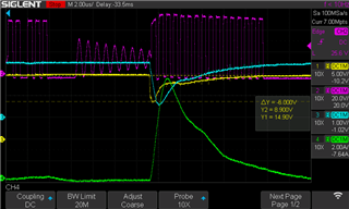
1. Why input voltage ( normally 48V) goes higher than 48V? visible in Pink curve on SWT pin ( and fig 5 blue) it goes higher aboy 3V than the input voltage.
Seem like some energy is back transferred somehow to the input cap C31 cap. The only possible source of this voltage increase is L1, but how? there is inside reverse polarized diode, which seems to be fine, after MM diode test.
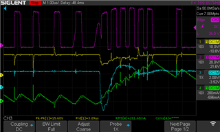
2. Why the LM goes not off due to the UVLO? voltage on Vcc caps(7V reg) goes down to 1V, fig 3, it is still switching SWT pin, why?.
circuit

Fig1
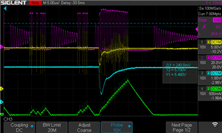
Legend; fig1:fig4
Pink SWT,
blue Vcc (7V),
green Inductor current,
yell Vout (15V)

fig2
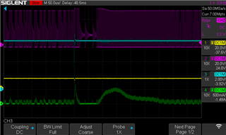
fig3
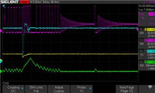
fig5
Blue- Vin (48V)
yll- SWT
pink - high side mosfet Q1 gate
green inductor curent