This thread has been locked.

If you have a related question, please click the "Ask a related question" button in the top right corner. The newly created question will be automatically linked to this question.

TPS53688: The D-CAP+TM Bode Plots Measurement Setup and Gain Margin Value

Part Number: TPS53688

Hi,

My question as below:

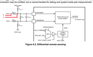
1. The D-CAP+TM Bode Plots Measurement Setup

    What is the correct amplitude and point of signal injection for TPS53688?

2. What is the reasonable gain margin for D-CAP+ TM control system?

    Based on TI technical document paper "Slup 173", it recommend the gain margin value as -6 dB to -12 dB.

    But for the D-Cap+ TM control system, when we try to improve the transient response the gain margin normally around -3 dB to -6 dB.

    Then we do need to sacrifice the transient response for -10 dB gain margin.

    But customer is not happy with it.

    Therefore we do need TI help to explain it.

     BTW, I saw another TI technical document paper  https://e2e.ti.com/blogs_/b/powerhouse/posts/the-d-cap-modulator-evaluating-the-small-signal-robustness

     Base on it's figure 1,2 & 3, (Bode Plots Curve) which gain margin is less than -10 dB.

     Based to my understanding of -10 dB gain margin is to ensure that power supplies produced in large quantities will all be stable, and rsubain that way throughout their lifetime.

     This allows parameter changes which could cause the loop gain to change by a factor of approximately 3 before the system becomes unstable.

     But as TPS53688 it is digital control and without a lots of R and C device for loop gain compensation.

     Therefore, my question is for D-cap + TM what is the reasonable gain margin value is?

  • 1- Please refer to the sketch below. 

    2- Typically we recommend at least -6dB gain margin for DCAP+ converters. 

    Also, while the TPS53688 allows compensation tuning through I2C/PMBus, it is still an analog control loop. Like when you change the DC Load line (VOUT DROOP), the device adjusts an internal resistor DAC, instead of an external resistor. 

  • Hi Matt,

    Thanks for your quick feedback.

    BTW, your feedback do answer my question but the tough thing still exist.

    To achieve -10 dB gain will sacrifice the transient response.

    And the I2C/PMBus compensation tuning of TPS53688 is difficult to understand how to deal with.

    For example, the traditional analog control is to tuning the DC gain, the frequency of pole and zero ...

    But TPS53688 I2C/PMBus compensation_CONFIG parameter is Vout_Droop, ACLL, DCM INC TC, DYN INT TC, INT TC and RAMP ...

    I can't understand how to deal with those parameters to achieve  my goal.

    Can you help to show me related technical document or TI website tool ?

    BTW, Can TPS53688 to do the compensation just like analog to add one more pole to adjust the gain margin ?

  • Please email me offline, and I can send a short pptx explaining the compensation parameters. Mjschurmann (at) TI (dot) com

  • Hi Matt,

    I don't know where to find your E-mail address.

    May you mail me your E-mail address?

  • My email address is : mjschurmann (at) ti (dot) com 

    You can also send the request to Vr@list.ti.com