This thread has been locked.

If you have a related question, please click the "Ask a related question" button in the top right corner. The newly created question will be automatically linked to this question.

UCD3138A: UCD3138A at resonant mode, the PWM0B sometimes is good, some times is HI level.

Part Number: UCD3138A
Other Parts Discussed in Thread: UCD3138, UCD3138064,

Hello,

I am using UCD3138ACCEVM149, ready to drive a LLC circuit.

I modified the demo program from trainingLab 3. 

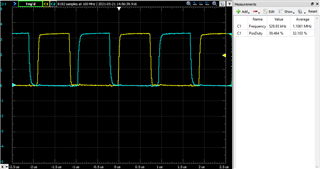
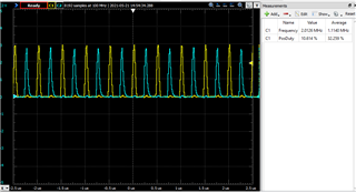
by changing the cpusample value, i can see the output PWM signal changing from 500KHz to 2MHz, that is working as I expect (PWM0 module).

while the problem is 

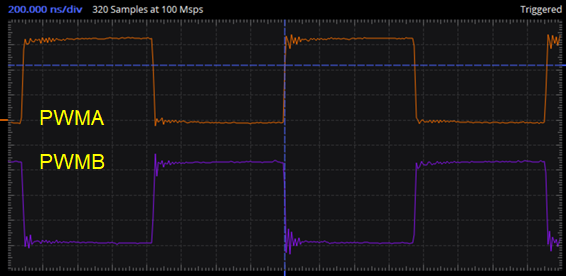
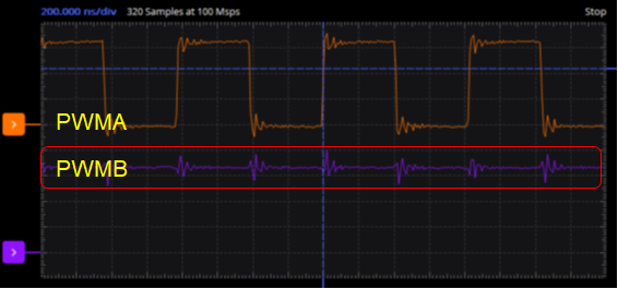
PWM0A pin is always good, 

but the PWM0B sometimes is good, some times is HI level. 

I mean during the frequency of 500kHz ~ 2MHz, Pwm0B is good at some frequency, but output HI level at some other frequency.

I am confused, 

would you please give me some advices on what could be the reason of it? 

thanks a lot!

Xioafeng Wu

  • Hi Xioafeng,

    Are you using the UCD3138ACCEVM149 with the LLC EVM ( https://www.ti.com/tool/UCD3138ALLCEVM150 )?

    It will be difficult to debug the issue without knowing the changes to Lab03. It might be easier to start with the LLC EVM firmware ( https://www.ti.com/tool/UCD3138FW_LLC ).

    Regards,

    Swami

  • Hi, 

    thank u for the quick answer, 

    I am using only the UCD3138ACCEVM149, without EVM150. 

    So, as I start with the UCD3138FW_LLC, it can`t work because of no input of proper voltage etc.

    one of your colleague suggested I should start with the trainingLABs, that is the story.

    following is my code, would you please have a look on it?

    **********************************************************

    //###########################################################################
    //
    // FILE: main.c
    //
    // TITLE: main
    //
    // NOTES:
    // 1)

    //###########################################################################
    //
    // Ver | dd mmm yyyy | Who | Description of changes
    // ======|=============|======|==============================================
    // 1.00 | 05 May 2021 | CH |
    //
    // Texas Instruments, Inc
    // Copyright Texas Instruments 2008. All rights reserved.
    //###########################################################################
    #define MAIN 1

    #include "system_defines.h"
    #include "Cyclone_Device.h"
    #include "pmbus_commands.h"
    #include "pmbus_common.h"
    #include "pmbus_topology.h"
    #include "variables.h"
    #include "functions.h"
    #include "software_interrupts.h"
    #include "cyclone_defines.h"
    #include "stdio.h"

    #define PCLK_PERIOD 4.0e-9 //base clock 4ns, Hi resolution clock 250ns
    #define PERIOD_SECONDS 2e-6 //Min Frequency 500kHz, Max Period 2us
    #define PERIOD ((int)(PERIOD_SECONDS/PCLK_PERIOD)<<4) // 500*16 = 8000 250ns/1
    #define EVENT1 (int)(PERIOD*0) // 0
    #define EVENT2 (int)(PERIOD*0.4) // 3200 0.8us
    #define EVENT3 (int)(PERIOD*0.5) // 4000 1.0us deadtime1 = 0.2us
    #define EVENT4 (int)(PERIOD*0.9) // 7200 1.8us deadtime2 = 0.2us

    int ram_cpu_sample;
    // comment for hyperknob [min=0, max=255, step=8]

    void init_dpwm0(void)
    {

    Dpwm0Regs.DPWMCTRL0.bit.PWM_EN = 0; //disable locally for init
    Dpwm0Regs.DPWMCTRL0.bit.CLA_EN = 1; //default is 1 - use cla

    Dpwm0Regs.DPWMPRD.all = PERIOD; // use .all for all values, so that the scaling matches
    Dpwm0Regs.DPWMEV1.all = EVENT1; // set EVENT 1
    Dpwm0Regs.DPWMEV2.all = EVENT2; // set EVENT 2
    Dpwm0Regs.DPWMEV3.all = EVENT3; // set EVENT 3
    Dpwm0Regs.DPWMEV4.all = EVENT4; // set EVENT 4

    Dpwm0Regs.DPWMCTRL2.bit.SAMPLE_TRIG_1_EN = 1; //enable 1 sample trigger
    Dpwm0Regs.DPWMCTRL1.bit.EVENT_UP_SEL = 1; //update at end of period
    // Dpwm0Regs.DPWMCTRL0.bit.PWM_MODE = 0; //normal mode (this is NOT the default)
    Dpwm0Regs.DPWMCTRL0.bit.PWM_MODE = 1; //resonant mode (edit by Wu 20210514)

    Dpwm0Regs.DPWMCTRL0.bit.CBC_ADV_CNT_EN =0 ; //Selects cycle-by-cycle of operation changed to 0 by Wu
    // Normal Mode
    // 0 = CBC disabled (Default)
    // 1 = CBC enabled
    // Multi and Resonant Modes
    // 0 = PWM-A and PWM-B operate independently (Default)
    // 1 = PWM-A and PWM-B pulse matching enabled
    Dpwm0Regs.DPWMCTRL1.bit.HIRES_DIS = 0; //0 = Enable High Resolution logic
    Dpwm0Regs.DPWMCTRL1.bit.CHECK_OVERRIDE = 0; //Disable math checks, there is a bug in the hardware


    //Set duty to filter as pwm-per-adj reg
    Dpwm0Regs.DPWMCTRL2.bit.FILTER_DUTY_SEL = 2; //(add by Wu 20210517)
    //0 Maximum Filter output gives 100% duty cycle
    //1 Maximum Filter output gives Event 2 duty cycle
    //2 Maximum Filter output gives value of Resonant Duty Register (for LLC)
    //3 Not applicable

    Dpwm0Regs.DPWMPHASETRIG.bit.PHASE_TRIGGER = 0; //8nsec phase delay //change to 0 by Wu

    //Dpwm0Regs.DPWMSAMPTRIG1.all = (PERIOD * 3)/4; //3/4 of period
    Dpwm0Regs.DPWMSAMPTRIG1.all = 32; //(add by Wu 20210517)

    Dpwm0Regs.DPWMPRD.all = PERIOD;

    /*The register RESONANT_DUTY is used in LLC topologies to produce the correct Filter Duty output. The Filter output is
    multiplied by this register to calculate Filter Duty. In the LLC reference firmware (UCD3138LLCEVM-028) it
    is set to 1/2 of the maximum desired period. In this case, bits 13-0 are used as an unsigned number. To
    enable this mode, the DPWM must be in Resonant Mode, and the FILTER_DUTY_SEL field in
    DPWMCTRL2 must be set to a 2.*/

    Dpwm0Regs.DPWMRESDUTY.bit.RESONANT_DUTY=((PERIOD >> 4) + 1 ) >> 1; //
    //This register is used in LLC topologies to produce the correct Filter Duty output.
    //The Filter output is multiplied by this register to calculate Filter Duty.
    //

    // as a Filter Output Multiplier in Resonant Mode.
    Dpwm0Regs.DPWMCTRL0.bit.MIN_DUTY_MODE = 0;

    Dpwm0Regs.DPWMCTRL0.bit.CBC_PWM_AB_EN =1 ; //Sets if Fault CBC changes output waveform for PWM-A and PWMB
    //0 = PWM-A and PWM-B unaffected by Fault CBC (Default)
    //1 = PWM-A and PWM-B affected by Fault CBC

    Dpwm0Regs.DPWMCTRL1.bit.CBC_BSIDE_ACTIVE_EN =1 ; ///Sets if CBC responds to Fault CBC when PWM-B is active,
    // only available in Multi and Reson modes
    // 0 = Response to Fault CBC when PWM-A active (Default)
    // 1 = Response to Fault CBC when PWM-A or PWM-B active

    Dpwm0Regs.DPWMCTRL1.bit.GLOBAL_PERIOD_EN = 1;
    Dpwm0Regs.DPWMCTRL0.bit.PWM_EN = 1; // enable DPWM0 locally
    }

    void init_filter0(void)
    {
    // special set up for CPU SAMPLE - all coefficients are zeroed except for P.
    Filter0Regs.FILTERCTRL.bit.USE_CPU_SAMPLE = 1; // enable CPU Sample

    Filter0Regs.FILTERCTRL.bit.FORCE_START = 1; // Initiates a filter calculation under firmware control
    // 0 = No calculation started (Default)
    // 1 = Calculation started

    Filter0Regs.CPUXN.bit.CPU_SAMPLE = 34; // set to 1/4
    //----------------------------------------------------------------------------------
    // lab 3 tasks:
    // place values on the three filter coefficients (KP, KI and KD) and Kalpha
    // - initialize Kp so as Xn passes through the proportinal branch unchanged
    // - initialize Ki and Kd as the the integral and differential branches are disabled
    // - initialize Kalpha so as the Kalpha pole has no influence on the differential branch
    // place value on the integrator KDALPHA coefficient also
    //----------------------------------------------------------------------------------
    Filter0Regs.FILTERKPCOEF0.bit.KP_COEF_0 = 0x7fff; //full pass through of XN value.
    Filter0Regs.FILTERKICOEF0.bit.KI_COEF_0 = 0;
    Filter0Regs.FILTERKDCOEF0.bit.KD_COEF_0 = 0;
    Filter0Regs.FILTERKDALPHA.bit.KD_ALPHA_0 = 0;


    Filter0Regs.FILTERYNCLPHI.bit.YN_CLAMP_HIGH = 0x799999; // 95% max duty 0.95us = 47.5% 500kHz
    //Filter0Regs.FILTERYNCLPHI.bit.YN_CLAMP_HIGH = 0x199999; // 20% max duty
    //Filter0Regs.FILTERYNCLPLO.bit.YN_CLAMP_LOW = 0x0; // 0% min duty
    Filter0Regs.FILTERYNCLPLO.bit.YN_CLAMP_LOW = 0x1FFFFF; // 25% min duty 0.25us = 12.5% 2MHz

    Filter0Regs.FILTEROCLPHI.bit.OUTPUT_CLAMP_HIGH = 0x3FFFF;
    //Filter0Regs.FILTEROCLPHI.bit.OUTPUT_CLAMP_HIGH = 0x0CCCC; // 20% max duty
    Filter0Regs.FILTEROCLPLO.bit.OUTPUT_CLAMP_LOW = 0; // 0% min duty

    //Setup connection for max duty/period into Filter.

    Filter0Regs.FILTERCTRL.bit.PERIOD_MULT_SEL = 1; //(add by Wu 20210517)
    //Input to filter for DUTY max comes from DPWM
    Filter0Regs.FILTERCTRL.bit.OUTPUT_MULT_SEL = 3;

    Filter0Regs.FILTERCTRL.bit.OUTPUT_SCALE = 0; /// no shift

    Filter0Regs.FILTERCTRL.bit.FILTER_EN = 1;
    //enable OK here, because nothing will happen until DPWM and front end are globally enabled

    // Filter0Regs.FILTERCTRL.bit.OUTPUT_MULT_SEL = 1; // use period for output multiplier.


    // Better option for handling shoot through - uses full dynamic range of filter
    // LoopMuxRegs.FILTERKCOMPA.bit.KCOMP0 = (PERIOD/2) >> 4; // KCOMP is at 4 ns, period is at 250 ps
    // Filter0Regs.FILTERCTRL.bit.OUTPUT_MULT_SEL = 0; // select half period kcomp for output multiplier
    }

    void init_loop_mux(void)
    {

    LoopMuxRegs.FECTRL0MUX.bit.DPWM0_FRAME_SYNC_EN = 1; //Enables DPWM Trigger from DPWM 0 Frame
    //Sync to Front End Control
    //0 = DPWM 0 Frame Sync not routed to Front End Control (Default)
    //1 = DPWM 0 Frame Sync routed to Front End Control


    //Set which DPWMs output connects to the filter as an input
    //DPWM-0 connects to filter for resonant duty
    LoopMuxRegs.FILTERMUX.bit.FILTER0_PER_SEL = 0; //(add by Wu 20210517)

    //Set filter KCOMP value (which is the maximum PERIOD)
    //Use value in KCOMP-0 register
    LoopMuxRegs.FILTERMUX.bit.FILTER0_KCOMP_SEL = 0; //(add by Wu 20210517)
    //Input to filter for PERIOD max comes from LOOP MUX (KCOMP)
    LoopMuxRegs.FILTERKCOMPA.bit.KCOMP0 = (PERIOD) >> 4; // KCOMP is at 4 ns, period is at 250 ps KCOM = period
    LoopMuxRegs.PWMGLBPER.all= PERIOD;

    LoopMuxRegs.DPWMMUX.bit.DPWM0_FILTER_SEL = 0; // use filter 0 for DPWM 0

    //Connect filter 0 to front end 0
    LoopMuxRegs.FILTERMUX.bit.FILTER0_FE_SEL = 0; //(add by Wu 20210517)

    LoopMuxRegs.SAMPTRIGCTRL.bit.FE0_TRIG_DPWM0_EN = 1; // use DPWM0 for filter0 sample trigger
    }

    void global_enable(void)
    {
    union GLBEN_REG glben_store; // collect global enable bits for simultaneous use
    glben_store.all = 0;
    glben_store.bit.DPWM0_EN = 1;
    glben_store.bit.FE_CTRL0_EN = 1;
    LoopMuxRegs.GLBEN = glben_store;
    }

    void main()
    {
    // enable JTAG
    MiscAnalogRegs.IOMUX.all = 0;

    //---------------------------------------------------------------------------
    // IMPORTANT: READ BELOW, OR CODE MAY NOT EXECUTE CORRECTLY
    //---------------------------------------------------------------------------
    // tie pin FAULT3 to ground for normal operation
    // tie pin FAULT3 to 3.3V to clear checksum
    if(GioRegs.FAULTIN.bit.FLT3_IN == 1)
    {
    clear_integrity_word();
    }

    #if (UCD3138|UCD3138064)
    MiscAnalogRegs.CLKTRIM.bit.HFO_LN_FILTER_EN = 0;
    MiscAnalogRegs.CSTRIM.bit.RESISTOR_TRIM =23; //28;
    #endif

    init_pmbus(0x58); // initialize PMBus handler
    init_dpwm0(); // initialize DPWM0
    init_filter0();
    init_loop_mux();
    global_enable();
    ram_cpu_sample = Filter0Regs.CPUXN.bit.CPU_SAMPLE; // initialize hyperknob
    for(;;)
    {
    pmbus_handler();
    Filter0Regs.CPUXN.bit.CPU_SAMPLE = ram_cpu_sample; // put hyperknob value into register
    }
    }


    //#pragma INTERRUPT(c_int00,RESET)

    void c_int00(void)
    {
    main();
    }

    **********

    ****************************************************

    with regards!

    Xiaofeng

  • Hi Xiaofeng,

    Thanks for the code. I am trying to duplicate your issue. Let me check and update you tomorrow.

    Regards,

    Swami

  • Hi Swami

    Thanks a lot, looking forward for your result.

    Regards

    Xiaofeng

  • Hi Xiaofeng,

    I ran your code many times, but I could not duplicate the issue. Here are my results (Blue line is 0A, Yellow line is 0B):

    ram_cpu_samples = 255:

    ram_cpu_samples = 0:

    As you can see the signals appear to be normal. I did not see an instance where the 0B stayed high in my case.

    There are only a couple of other reasons I can think of for this issue:

    1. There is a section of code to recover from lockup condition:

    //---------------------------------------------------------------------------
    // IMPORTANT: READ BELOW, OR CODE MAY NOT EXECUTE CORRECTLY
    //---------------------------------------------------------------------------
    // tie pin FAULT3 to ground for normal operation
    // tie pin FAULT3 to 3.3V to clear checksum
    if(GioRegs.FAULTIN.bit.FLT3_IN == 1)
    {
        clear_integrity_word();
    }

    If the FAULT3 is not tied to ground, the code can reset and it might look like 0B is staying high. Can you lease check if FAULT3 is tied to ground?

    2. There is some issue in the hardware. Is it possible to try another EVM if you have it?

    Regards,

    Swami

  • You mention that it fails at some frequencies but not at others.  Can you give us the exact sequence for both a successful and an unsuccessful run?  Are you changing the frequency in the code or using the memory debugger?  

  • HI, Swami

    thank your so much for the confirmation. It surprising me that the code works well on your EVM-board.

    as for you question:

    1.Of course I tied FAULT3 to ground, if not the code cannot work to output angthing.

    2. It will cost several days for me to get another EVMboard.

    So, to confirm the hardware problem, I wonder if you can send me the .x0 file that you download in EVM, that would be very helpful.

    and here is the wave forms for the issue.

    By the way, I found another problem.

    in my case, even when the PWM0B is good, the deadtime looks like to be zero, that is also different from your result.


  • HI, Bower

    thank you again!

    I paste 2 waveforms at the reply upper, hope it will help you to understand my issue.

    I always changing the frequency in the memory debugger of UCD3xxx GUI.

    I am wondering, if the code is the same, and no problem on hardware, the building configuraion could be the reason. 

    do you got any other idea?

    with regards!

    Xiaofeng

  • Xiaofeng, can you tell me a specific value you load into the memory debugger that consistently causes PWMB to stay low, and a value that consistently load that always works?  That way I won't have to search.  Also tell me what register you are writing to.  And are you writing to the bitfield or the .all(the whole register)?  I don't believe that the overall compilation settings will have an effect.  Unless you are using the UCD3138 settings instead of the UCD3138A.  You may want to right click on the project in CCS and select show Build settings.  Click on General a the top of the list, and you will see Configurations.  Click on Manage configurations, and make the UCD3138A the active configuration and rebuild the project.  I don't know if that will make a difference or not, but if you are compiling for UCD3138, it may help to switch to the UCD3138A configuration.  

  • Hi, Bower

    thanks a lot, actually I found the reason. that would thanks for your remainding that UCD3138A is different from UCD3138.

    then I found the following information

    That means all the deadtimes in UCD3138A were decided by EVENT_1.  As the EVENT_1 in my code was set to 0,  so the deadtime Δ1~4 are all 0. That makes the down edge of PWM0A in the same time of up edge of PWM0B. And the time error will decide PWM0B shoot-though or not.

    So, when I modifide the code as following, the problem was fixed.

    #define EVENT1 (int)(PERIOD*0.1)

    Thank you for your support!

    Xioafeng