


Hello all,
I am designing a system that takes power from an input supply and generates a negative and positive supply voltage for biasing op amps. I created a test setup, but I am getting some odd results.
Design Brief:
- input power regulated switching power supply (will eventually be USB bus power)
- 5V in, regulated to + and - 3.3V
- Must be able to handle current of 800mA (maybe 1A max) through positive regulator
- Must be able to handle current of 40 mA through negative regulator
- noise level of less than 1 mVpp
See the following schematic:
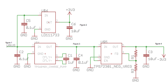
When loaded with active devices (analog to digital converter, four op amps, etc.) and drawing about 91 mA current, the waveforms observed are as follows (labels on schematic correspond to waveforms below):

Figure 1
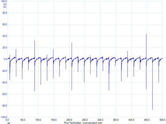
Figure 2

Figure 3 (inverter supplying about 17 mA)
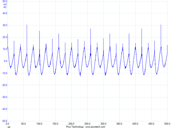
Figure 4
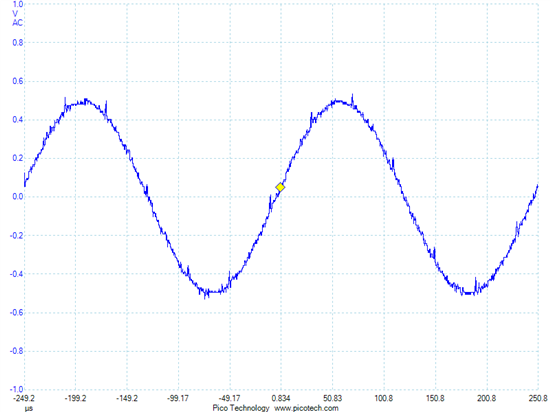
These noisy waveforms feed into the signal stage and cause a great deal of noise on the signal (see above figure). I have an instrumentation application, so I need to figure out how to get rid of this noise completely. My analysis indicates that the inverting switched capacitor circuit is a very problematic element. I have heard that the 250 kHz fixed version of the TPS6040X has better noise performance under load.
Does anyone have suggestions on how to go about fixing this problem? I would like two low noise LDOs, one for positive and one for negative voltage regulation, as well as to generate the negative voltage from the switching capacitor IC.
Thanks,
Alex

