This thread has been locked.

If you have a related question, please click the "Ask a related question" button in the top right corner. The newly created question will be automatically linked to this question.

LM5116: LM5116 IC failure

Part Number: LM5116

Hi 

As a continuation to the previous query

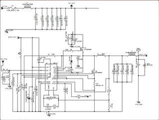
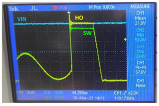
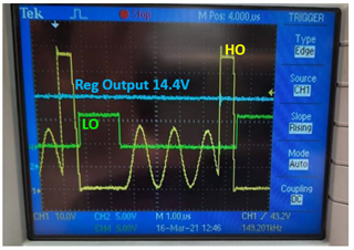
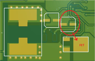
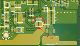
"We have used LM5116 PMIC to output 14.4V/3A from max input of 60V in our product design. 

PMIC is repeatedly failing with failure mode of output 0V. When debugged Pins HB, HO,SW Impedance always found to be low [some cases shorted to GND potential]"

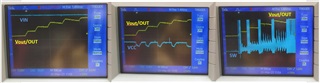
We have waveforms of a partially failed LM5116 IC [found HB and SW pin with low impedance than expected]

All signals measured wrt board GND potential [14.4V regulated output, VIN, VCC, SW node pin]

Attached the waveforms.

Please revert back on the  possible failure mode

  • Hi Mutum,

    Please send the schematic, layout and a completed LM5116 quickstart file for this design. Also, what is the MOSFET part number?

    Regards,

    Tim

  • Hi Timothy,

    Please find the Sch, Layout and quickstart file attached.

    MOSFET MPN -SUD80460E-GE3

     8080.LM5116_quickstart_shared.xlsx

    2L PCB
    Bottom layout: IC and peripherals

    Top layout: Inductor

  • Hi Mutum,

    This MOSFET has very high Qrr and will likely produce noisy switching waveforms. No need for a 150V FET for a 60V max Vin. Also, the input caps should be close to the FETs (see app note snva803 for more detail). The high-side gate traces are a bit long and narrow as well.

    Can you send the SW and gate drive voltage waveforms (HO minus SW is the high-side gate) at 60Vin and full load.

    Regards,

    Tim

  • Hi

    The Qg of the selected MOSFET is very Low.

    The inputs caps are placed near the MOSFETs (highlighted circle is the input caps and FETs locations in the below layout image)

    The below are gate, SW node waveforms at normal load (all signals wrt ground potential)

  • Hi Mutum,

    The VCCX should be powered by a high enough voltage to drive the FETs (5V is not enough). The gate drive amplitude should be at least 2V above the Miller plateau of the FET.

    It's always better to have the power stage on one layer to avoid via inductance contribution. Also, as the controller is a bit far from the FETs, check that the gate traces HO and SW are routed together as a diff pair. Finally, you can reduce the boot cap to 0.1-0.22uF (the VCC cap should be 5-10x the boot cap such that the VCC rail is not excessively discharged when the boot cap is initially charged at startup).

    Regards,

    Tim