This thread has been locked.

If you have a related question, please click the "Ask a related question" button in the top right corner. The newly created question will be automatically linked to this question.

TPS2663: TPS2663X priority power MUX

Part Number: TPS2663

I want to use two TPS2663X eFUSEs for priority power muxing of two 28VDC supplies.

In section 10.3.2 of the data sheet the following is stated "The TPS2663x devices provide a simple solution for priority power multiplexing needs."

However, when looking at Figure 53, I can see that the OVP pin is required, which is only present for the TPS26630 and TPS26631 devices.

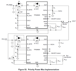
This must mean that priority muxing is not supported by the TPS26632/TPS26633/TPS26635/TPS266336?

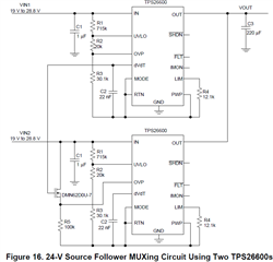
This is also what I can gather from application note SLVA811A - "Power Multiplexing Using Load Switches and eFuses", Figure 16.

Can you please explain the working of the circuit in Figure 53?

How should the resistor R8 be calculated?

Regards Lars

  • Thanks for reaching out to us.We will get back to you by Monday, 24-May-21.

  • Hi Lars,

    Yes, only TPS2663x variants having OVP pin supports power-muxing operation.

    Circuit function: Under normal operation, if VIN_MAIN is present, the primary eFuse turns on. When the primary eFuse is operating, the dVdT(Primary eFuse) is typically 4.17 V.  The voltage across R8 will be 4.17V-Vth(Q5) which is higher than OVP threshold of 1.2V. This keeps the internal FET of the secondary eFuse disabled. You can select R8 in the order of 100k to 1000k to minimize the shunt current from VIN_AUX

    Best Regards,

    Rakesh

  • Hi Rakesh

    I am sorry, but the function, as you describe it, isn’t clear to me.

    As I see it dVdT of the primary eFUSE is connected to the gate of Q5, which is a logic level N-channel MOSFET working as a switch. The drain of Q5 is at VIN_AUX potential and the source of Q5 is connected to R8. Assuming that the gate of Q5 and the OVP pin of the secondary eFUSE are high impedance, the voltage at the OVP pin would be pulled either down to GND (if Q5 acts as an open switch due to “low” voltage on the gate) or pulled up to VIN_AUX (if Q5 acts as a closed switch due to a “high” voltage on the gate). If the dVdT pin is at 4.17V when the primary eFUSE is operating, this would mean a closed switch and hence 24V on the OVP pin, which in turn turns off the internal FET of the secondary eFUSE. When the primary eFUSE isn’t operating, the dVdT pin is at 0V, meaning an open switch which in turn turns on the internal FET of the secondary eFUSE. Is my understanding correct or am I missing something?

    Regards

    Lars

  • Hi Lars,

    The gate of Q5 has two states, zero when primary eFuse is off and 4.17 V (typical) when primary eFuse is on. Therefore, when primary eFuse is on, dVdT pin of this eFuse and gate of Q5 are at 4.17 V (typical). Hence, OVP pin of secondary eFuse becomes 4.17 V - VGSth (Gate Threshold Voltage) of Q5, not the input of this eFuse (24 V) because Q5 is operating in common drain amplifier configuration here. This makes secondary eFuse turned off because OVP pin of this eFuse is at greater than 1.2 V (Overvoltage Threshold Voltage). During the power failure at primary eFuse, dVdT pin of this eFuse will going to be 0 V, which makes Q5 turned off and OVP pin of secondary eFuse pulled low to ground through R8. This enables the secondary eFuse and then load is taking care by this eFuse. 

    Please click on "This resolved my issue" if this post answers your query.

  • Thank you for the explanation, the function of the circuit is now clear to me. Which parameters are important when choosing an NMOS for Q5? I would mean that Vds should be rated to VIN_AUX or higher and that Vgs(th) should be less than 4.17-1.2V. An example could be BSS138 with Vds of 50V and and Vgs(th) of max 1.5V. Correct?

  • Hi Lars,

    Yes, you are correct.