This thread has been locked.

If you have a related question, please click the "Ask a related question" button in the top right corner. The newly created question will be automatically linked to this question.

UCC28704: Frequency and Amplitude modulation modes

Part Number: UCC28704
Other Parts Discussed in Thread: UCC28730

Hi E2E,

Figure 15 shows the four regions of operation. In region 3 the switching frequency is held constant (25kHz) while the peak current in the switch at turn-off is controlled from 25% to 100% of its maximum. In this region, our customer converter displays have some low-frequency oscillation in Vout (200mV p-p sinewave on +12Vdc with frequency ~500Hz).

Does stability in this region rely on the down-slope of the signal at Vs (pin 6) during the magnetizing reset time of Fig 14? If "yes", what is the range of slope to ensure good stability?


Regards,
Carlo

  • Hello Carlo,

    Stability of the UCC28704 flyback controller does not depend on the down-slope of the VS signal during demagnetization.
    It is important to maintain a relatively sharp knee point after the demagnetization interval where VS is sampled as in Figure 13.
    A "soft" knee, such as may be incurred from stray capacitance appearing on VS, may introduce a slight variation in sampling from one cycle to another, which may result in the 500Hz oscillation your customer observes. 

    I suggest to review the pcb layout at the VS input to ensure minimum trace lengths and minimal capacitance to GND and to other signals.
     

    Regards,
    Ulrich

  • Hello Ulrich,

    Thank you for looking into this. Our customer has the following concerns:

    My question pertains more to the stability criteria of these modes of operation, in particular: what part of the waveform at pin 3 influences stability in region 3. We are seeing 200mVp-p 300~500Hz sinewave on the +12Vdc output. We need noise and ripply voltage to be below 20mVp-p. What part of this waveform at Vs (pin6) will give us a clue as to what is the root cause of the AC ripple.

    I trying to get an overview of the UCC287xx family, ie: which devices have what features. The particular features I am interested in:
    1. primary side regulation (eliminates optos),
    2. ULVO thresholds >15V for on, <8V for off (to enable the device to directly drive MOSFET gates to about 10V peak).
    3. Valley switching (to reduce switching loss).
    4. Cable compensation - not required.

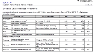
    These are all features of the UCC28704, however given my experience with this problem of instability, I would like to add another feature: that the Control Law output is available for observation. Ideally what I would like is the UCC28704 but in a 7 or 8 pin package with the analoge Control Law signal available at one of the extra pins. Does such a device exist? If not, is there a close relative that may suit? eg: the 28730.

    The unwanted oscillations on Vout (200mVp-p 300~500Hz sinewave) occur when we have 2 x 470u electro-caps on the output (refer schematic fragment, C5, C6). This problem stops when one of these electo caps is removed.

    When instability is present the pulse width and peak MOSFET current varies rapidly over a much wider range (from 1.42 to 3.89us) compared to when the ripple is not present. Attached waveforms show an example of both short and wide pulses, traces are:
    CH1 = Vsense winding
    CH2 = Vs (pin 6)
    CH3 = UCC28704 Vcc (pin 2)
    My ref: TEK0109, 0110.

    Comparing operation with and without the problem: I have not noticed any significant difference in the "knee" of Vs at end of de-mag period.

    If your hypothesis is correct, then what degree of knee "hardness" is necessary to ensure stability?

    The waveforms were taken at same load condition, which is at 259mA (about 25% of full load, in Region 3). Here are two more waveforms at longer time-base, taken under same line (200Vdc) and load conditions (+12V, 259mA), with the unwanted AC ripple present. One waveform is a short MOSFET on-time, the other is much longer on-time (my ref: TEK0099, 0100 resp).
    CH1= Vsense winding
    CH2= V cap of dv/dt snubber across Vsense winding
    CH3= UCC28704 Vcc (pin 2)
    CH4= MOSFET drain voltage

    The waveform of the output voltage when excessive ripple is occurring. Vout is nominally +12Vdc.
    This problem occurs when load is between 20% and 40% of full load (full load is 1.0A). It is not strongly dependant on input voltage.

    Please refer to the attached file.

    UCC28704.zip

    Your assistance is appreciated.

    Regards,
    Carlo

  • Hello Carlo,

    A 'scope probe itself on VS will add significant capacitance which may affect the knee characteristics.  The Vaux waveforms themselves show sufficient sharpness of the demag knee point for good stability.  Probing on VS can soften that knee, as well as shift the regulation voltage up slightly.  We strongly advise against putting a probe directly on VS; rather use the Vaux waveform and scale it by the resistor divider.  

    None of the UCC287xx family of flyback controllers have directly observable control laws. Operating points along the Law are inferred based on the actual Ippk and switching frequency compared to the maximum design Ippk and max design frequency at Iocc. 

    Given that the problem occurs for loads 20~40% of full load, I think the instability may be related to operating in the vicinity of the breakpoint between regions 3 and 4.  A small disturbance in sampling may push the operation either higher up the law or lower down the law, and delay in response can aggravate the disturbance into an oscillation. Removing one output cap seems to corelate to this, because the lower Cout makes a disturbance look larger and the loop can respond faster, avoiding an overshoot and squelching the tendency to oscillate. Perhaps using only 1 470uF cap is the solution to the stability issue.  Reducing output ripple to <20mV may require a trailing L-C filter stage, but it should be smaller than another 470uF cap.

    Regards,
    Ulrich

  • Hello Ulrich,

    Here is the response of our customer:

    Probing on VS can soften that knee, as well as shift the regulation voltage up slightly.  We strongly advise against putting a probe directly on VS; rather use the Vaux waveform and scale it by the resistor divider.  

    Yes, I am aware that this node (Vs) is sensitive to capacitance, including that of any probe. Be advised that our usual practice is to solder a leaded resistor (through-hole part, approx 1 to 2 kohm) to the node & attach scope probe to that resistor, which reduces the impact of any probe C. We used probes with tip C<15pF (x10, 200MHz).
    The behaviour of the device in regards to Vout ripple, and Vout regulation, remained the same regardless whether the scope probe was connected or not, which gives us confidence that scope probe did not significantly affect UCC28704 operation.

    Perhaps using only 1 470uF cap is the solution to the stability issue

    The problem is that one 470uF electro cap did not have the ripple current rating to give the required lifetime for this application. The original selection of 2x 470uF caps was driven by the need to ensure capacitor lifetime was not reduced by ripple current. Any given electro cap has an ESR value, and this contributes to self-heating caused by ripple current, which then contributes to temperature rise by the thermal impedance of the package (which is dependant upon the E-cap can size) and its installation (soldering to ground plane, air flow, proximity to heat sources, etc).

    Our concern is that if e-cap ESR affects stability, then we need to understand this issue so that we can take suitable steps to ensure stability over the entire range of operation, eg: select suitable caps, or introduce extra R.

    Reducing output ripple to <20mV may require a trailing L-C filter stage, but it should be smaller than another 470uF cap.

    Yes, our design already includes a trailing L-C filter stage, however its cut-off frequency (-3dB) is about 5kHz. It does reduce the ripple due to MOSFET switching to acceptable levels, however it does not filter out the low frequency ripple (300Hz to 500Hz) that we are seeing.

    Additionally, our customer is looking for Billy Long, and it seems he is no longer with TI as I checked with our directory.

    The reason I asked about Billy Long is because that is what came up when I searched for an overview of the UCC287xx device family.  So it would seem that I still do not have a document (say, a selection chart) that explains the devices in this family (the similarities and differences) that would allow easy selection of which member of the UCC287xx family would best suit a given application. 

    Here is one example of why this selection chart is important: the UCC28704 uses the sense winding to measure **both**:

    (a) Vout and (b) Vline. 

    To measure Vline the UCC28704 samples the current pulled out of the Vs pin when the MOSFET is on.  This current is set by the same resistors that set the voltage divider ratio used to set Vout, which also set the Vline start-up/shutdown voltage, refer datasheet parameters:

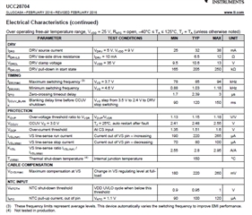
    IVSL(run)  VS line-sense run current  Current out of VS pin – increasing = 220μA typ

    IVSL(stop) VS line-sense stop current Current out of VS pin – decreasing = 80μA typ

    (Refer attached screenshots of relevant part of datasheet).


    Because of the multiple functions served by the Vs pin, the values of these resistors are not freely selectable (only a certain range of values fulfills all requirements).  In our case, these R values are quite high and result in a rather high impedance for the signal at the Vs pin, which then makes it sensitive to any stray C at that pin, which may be contributing to the problems we are seeing. 

    So what I would like to find is a member of the UCC287xx family that senses Vline differently, so that we can freely select the resistor values based only on setting Vout, so we can make the signal impedance at Vs lower to reduce effect of any C at the Vs (pin 6).  I was hoping there would be an easy-to-use selector chart for that purpose.  One member of this family that looked promising was the UCC28730 which has a separate connection to Vline (HV pin).  I had originally thought it was the solution to our problems because I thought it measured Vline via that HV connection.  Alas, upon closer reading of the datasheet I realised that it senses Vline in the same way as UCC28704, that connection to Vlne is only to power the chip for start up. 

    So my problem remains unsolved.

    Your further assistance is appreciated.

    Regards,
    Carlo

  • Hello Carlo, 

    All members of the UCC287XX family use the VS input for both output sensing and line voltage sensing (actually, bulk voltage sensing). With limited number of pins available, multi-function is necessary, which does constrain the choice of resistor values. 
    Those devices with the HV pin incorporate a high voltage JFET for faster start-up and lower stand-by power purposes only.  It does not perform any other function. 

    The stability of the PSR controllers does not depend on ESR of the output cap.  The sampling is chosen at the demag knee precisely because that is where the winding current goes to zero and the contribution of any ripple voltage from ESR is also zero.  In this sampling method, stability is mostly a matter of avoiding delays in the feedback path which would cause the controller to react to conditions which are already significantly in the past.  This is how low frequency ripple can be reinforced, because the loop is trying to compensate too late for an output change that has already gone in the other direction.  

    My concern about the extra 470uF cap is that it may causing Vout to change more slowly as the contol is trying to adjust for what it samples.
    I understand ripple current is a concern.  Perhaps two 220uF ~270uF caps can be used in parallel to share the current, since the two Cout positions are available. 

    Isolating a 15pF scope probe with only 2K in a network with 10's of Kohm impedance may not be enough to shield VS from it's filtering influence in all cases.  Since the circuit behaves the same even without the probe attached, I agree it can't be the probe causing a delay. 
    There is still the pcb layout stray capacitance to consider.  The design guidance is to locate both bottom and top resistors of the divider right at the pin to minimize track length and its subsequent capacitance.  
    To test for capacitance effects on VS, I suggest to reduce both VS resistors by 5~10X to reduce any RC time constant.  

    This will keep the regulation the same, but it will allow start-up at a much lower bulk voltage. That is irrelevant of test purposes, you can still apply the normal input to start.  If there is no improvement in the ripple, then I think reducing Cout may be the only recourse.  There is nothing else left to adjust. 

    One last thing, try shorting out the output inductor of the LC filter for test purposes.  If it is ringing with the 470's maybe you can change its value or add a damper across it.  If it has no effect then, we're back to the previous paragraph.  

    Regards,
    Ulrich

  • Hello Ulrich, 

    Here is the response of our customer:

    One last thing, try shorting out the output inductor of the LC filter for test purposes.  If it is ringing with the 470's maybe you can change its value or add a damper across it.  If it has no effect then, we're back to the previous paragraph.  

    We have already eliminated resonance between any of the output filter components as the root cause of this problem.

    My concern about the extra 470uF cap is that it may causing Vout to change more slowly as the contol is trying to adjust for what it samples.

    That suggests that stability is dependant the rate of change of Vout, which is dependant upon both C, and its ESR (which is simply time-constant). This means there is an upper value of C, and lower limit of ESR, beyond which instability may occur. Please share with us the information we need to calculate the dependency of stability margin on C and ESR.

    I understand ripple current is a concern.  Perhaps two 220uF ~270uF caps can be used in parallel to share the current, since the two Cout positions are available

    Yes, we have already explored this option. The problem is that parts must meet **all** the requirements for C, ESR, ripple current rating, and temperature. Taking all of these factors into account dramatically reduces the range of suitable components, and suitable parts are simply not available from our suppliers.

    If we had better understanding of what the limits are for C and ESR, then we could perhaps expand the range of suitable components, and hence have more luck sourcing them. As of now all we can do is go off what we know that works (eg 1 x 470uF) and select parallel caps to give the same C & ESR values.

    To test for capacitance effects on VS, I suggest to reduce both VS resistors by 5~10X to reduce any RC time constant.  

    Yes, it would seem that the only option remaining (apart from better understand of effect of C and ESR upon stability), is to do this test.

    Thanks for your help thus far.

    Regards,
    Carlo

  • Hello Carlo,

    A I mentioned before, since the UCC28704 samples VOUT (by way of VS) when the demag current has gone to zero, the ESR of the output cap plays no role in stability. ESR is still a factor in ripple voltage, but no need to match anything for stability.

    The stability criterion presented in the datasheet is Equation (5), page 14.  Both 1x470uF and 2x470uF meet this criterion.
    I found out another limitation: Cout > 3000~5000uF may lead to oscillation at 1.5kHz, but this is not affecting your design. 

    All face-value parameters say that your design should be stable.  Since it is not, there must be an unwanted and uncharacterized parasitic parameter in the design. I suspect that this parasitic is stray capacitance on the VS node, which can add a time-delay into the loop response.
    The observed oscillation is symptomatic of that time delay, in my opinion.
    Reducing Cout by half makes its Vout sampling twice as sensitive, because a change in duty-cycle based on the last sample can move Vout twice as much and be more easily detected on the next sample. This serves to damp out an oscillation due to time-delay.

    I look forward to the results of testing with greatly reduced Rvs1 and Rvs2 on VS while Cout = 2x470uF.


    Regards,
    Ulrich    

  • Hello Ulrich,

    Here is the response of our customer:

    I found out another limitation: Cout > 3000~5000uF may lead to oscillation at 1.5kHz, but this is not affecting your design. 

    Please share the formula to calculate the value of Cout that will cause this 1.5kHz oscillation. Is the value you quoted (3000~5000uF) dependant upon Vout? Please note that our design is for +12V, so I suspect this will mean that this will *reduce* the C value at which this oscillation will occur (the secondary winding and the sense winding have the same number of turns, so the turns ratio is 1:1).

    Regarding the 1.5kHz oscillation: I assume this value of Cout (3000~5000uF) is connected directly across Vout, without any series R or L. What values of resistance (R) & inductance (L) would be required in series with the C of 3000~5000uF to prevent this oscillation? Please share the formula to compute both (a) R value (assuming L=0) and (b) L (assuming R=0), given the parameters of:
    1. Vout
    2. Iout(max)
    3. C
    4. Turns ratio of Vout winding (secondary) to sense winding.

    Thank you.

    Regards,
    Carlo

  • Hello Carlo,

    Uli is out this week on vacation.  However, the Webench tool found at the following link can be used to check the designs transformers turns ratio based on input and output power requirements,

     https://www.ti.com/product/UCC28740?keyMatch=UCC28740&tisearch=search-everything&usecase=GPN#design-development

    Regards,

    Mike

  • Hi Mike,

    According to our customer, he has already used that design tool and it does not answer his questions. Do you have any further advice?

    Thank you.

    Regards,
    Carlo

  • Hi, Carlo,

    We need to wait until Uli gets back for further follow-up on this thread.

  • Hello Don,

    I will wait for Ulrich's further advice, Thank you.

    Regards,
    Carlo

  • Hello Carlo,

    There is no formula or equation that describes or predicts the potential 1.5kHz ripple oscillation on the output if Cout is excessively large.  This situation is an observed phenomenon that has not been mathematically analyzed.  It was uncovered on a 5-V output while investigating a different issue a long time ago and was only informally characterized.  As such, I agree that the value of the excess capacitance to avoid would scale with the output voltage and Sec-Aux turns ratio.  But as I mentioned earlier, this is not germane to customer's immediate issue.

    Previously I had suggested to experimentally reduce the VS resistor values by a factor of 10 to see if stray capacitance on the VS node may be the source of the 200mV, 500Hz oscillations. This would reduce any time constant delay to 1/10th. Was the customer able to perform this test?

    Also, please remove the leaded probe resistor from the VS node.  This 1~2K resistor was used by the customer to isolate the probe capacitance from VS, but the resistor itself can be adding capacitance and/or acting as a wire antenna and injecting noise into VS.
    The customer mentioned that the output ripple was there whether the probe was connected or not.  If the leaded resistor is affecting VS independently of the scope probe and is left in place, then one could draw the wrong conclusion about the source of the oscillation.   

    I hope the results of this test are positive (ie. no oscillations).

    Regards,
    Ulrich

  • Hello Ulrich,

    Our customer is still in the process of testing, Once the result is available, I will give an update.

    Thank you.

    Regards,
    Carlo

  • Hi Ulrich,

    I received an update from the customer as follows:

    Also, please remove the leaded probe resistor from the VS node.  This 1~2K resistor was used by the customer to isolate the probe capacitance from VS, but the resistor itself can be adding capacitance and/or acting as a wire antenna and injecting noise into VS.
    The customer mentioned that the output ripple was there whether the probe was connected or not.  If the leaded resistor is affecting VS independently of the scope probe and is left in place, then one could draw the wrong conclusion about the source of the oscillation.

    Regarding the issue of viewing the VS (pin 6) with a scope, we have tested the unit thoroughly under the following conditions:

    1. Leaded resistor in place and with scope probe attached (x10, ~15pF)
    2. Leaded resistor in place and with scope probe attached (x100, ~2pF)
    3. Leaded resistor in place and no scope probe attached.
    4. Leaded resistor removed and no scope probe attached.

    In each case, the behaviour of the unit was unchanged - the unstable behaviour remained.  Therefore we concluded that our method of probing the VS pin had no effect on the unit.

    Previously I had suggested to experimentally reduce the VS resistor values by a factor of 10 to see if stray capacitance on the VS node may be the source of the 200mV, 500Hz oscillations. This would reduce any time constant delay to 1/10th. Was the customer able to perform this test?

    We understand the motivation for this proposed solution, however, we did not go down this path for two reasons:

    1. We decided this solution would not be acceptable, since it would have caused the unit to not meet the requirements regarding line voltage start-up and shutdown thresholds. The PCB was already laid out to minimize stray capacitance and could not be improved without resorting to exotic (& expensive) materials. If it was a "solution" then it would have required us to select a new IC anyway.
    2. We spent our time and effort exploring other solutions - we eventually found it: a 22pF capacitor placed across CS (pin 4) & GND (pin 5). I have other questions related to this solution which I will ask in a separate post.

    There is no formula or equation that describes or predicts the potential 1.5kHz ripple oscillation on the output if Cout is excessively large.  This situation is an observed phenomenon that has not been mathematically analyzed.  It was uncovered on a 5-V output while investigating a different issue a long time ago and was only informally characterized.  As such, I agree that the value of the excess capacitance to avoid would scale with the output voltage and Sec-Aux turns ratio.  But as I mentioned earlier, this is not germane to customer's immediate issue.

    Please share as much information about this problem as you can. Our application may be very similar to what revealed this problem to you, because in our case the output capacitance may be quite large. In our application, this unit will supply several PCA modules in a rack via a common +12V bus, and each PCA adds its own filter capacitance to the total capacitance seen by this unit. If some series R or L is required with each PCA to ensure stability, then we need to understand this so we can take the steps necessary to ensure stability under all possible combinations of which PCA cards are installed and their operating conditions.

    We have found a solution: a 22pF capacitor placed across CS (pin 4) & GND (pin 5). No other changes were necessary.
    This has eliminated all the unstable behaviour.

    However, I now have other questions related to this solution.
    1. RLC (connected to CS) was calculated from datasheet eqn 4 (or 3?) to be 2.2k (refer attached screenshot). Please confirm that the units used are all standard SI units, eg: volts, ohms (not kilo-ohms), seconds (not nano-seconds), henry (not micro-henry).

    2. What would be the consequences of making the value of RLC either (a) too low, or (b) too high?

    Thank you for the assistance.

    Regards,
    Carlo

  • Hi Carlo,

    I'm glad that your customer found the solution to the instability issue.  I did not suspect that it was somehow related to the CS input, and frankly I don't really understand why it would be true.  Usually a small cap is added to the CS input to filter leading-edge noise spikes which would prematurely cross the current sense threshold and shut off the gate drive.  Such noise (without Ccs) normally has a much worse effect on operation than a small (but unexplained) ripple on the output.  But the results speak for themselves.   

    To answer the new questions:
    1.  The units in equation (4) to calculate RLC are all standard SI units.
    2a.  RLC too low means insufficient CS offset at high line allowing higher Ippk and higher output current (power) at high line compared to low line.
    2b. RLC too high means too much CS offset at high line resulting in too low of Ippk and lower output current (power) at high line compared to low line. 

    An RLC value just right will result in a constant Iocc regulation (within ~5%) across the full line range. 

    Note: Introducing Ccs adds another delay term to be included in tD of equation (4).  With RLC=2.2K and Ccs=22pF, a filter time delay of 48ns is added and this will affect the ideal value of RLC.  Since the new time delay is a function of RLC, calculation becomes a bit iterative to converge on the proper value of RLC.  Since additional delay increases RLC, anticipate a higher RC time constant to add in to tD.  Generally a few iterations should get you close enough to maintain good Iocc regulation.  Empirical fine tuning can also be done during prototype evaluation.

    As regards the potential instability with very high Cout value, I'll need to dig deeper into it.  I'll reply as soon as I can.

    Regards,Ulrich