Hi All,
I have a question about TL494.
(1)
Please tell me the variation of 0.1V of Dead-Time Control Comparator in the block diagram below.
Also, what is the 0.7V variation of the PWM Comparator?

(2)
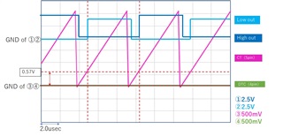
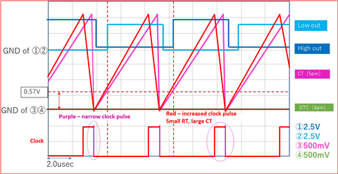
9.3.3 Please tell me about the description of Dead-time Control.
"An internal offset of 110 mV ensures a minimum dead time of ~ 3% with the dead-time control input grounded."
Although it is described like this, it was reported that it was about 10% when measured by the customer.
Why is the Dead-time 10%?
Best Regards,
Ishiwata