This thread has been locked.

If you have a related question, please click the "Ask a related question" button in the top right corner. The newly created question will be automatically linked to this question.

UCC28711: Low output frequency

Part Number: UCC28711
Other Parts Discussed in Thread: UCC27531

Hi!

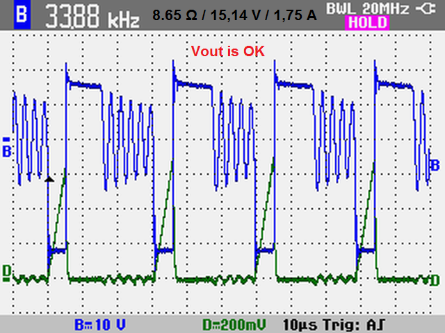
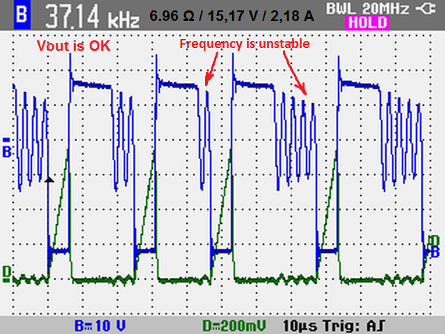
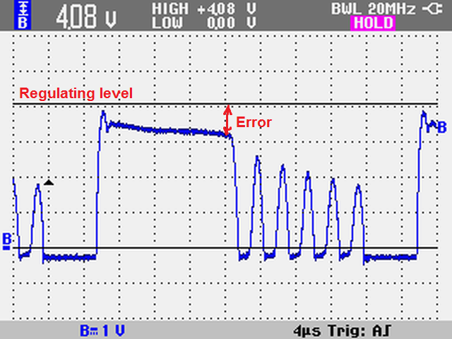
I designed 50 W flyback with 15 V output voltage. I have got quite a good regulation at loads up to 33 W. But when I connect extra load (total of 44 W) the power actually decreases as decreseses switching frequency and output voltage. Please see the waveforms (Red - Gate signal, Blue - Vaux voltage, Green - Vcs signal).

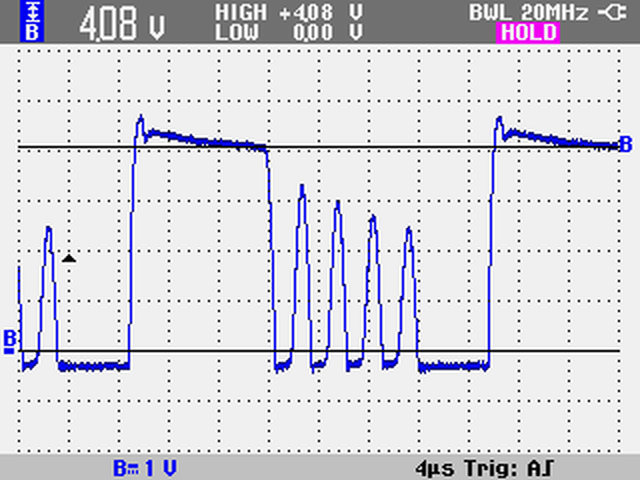
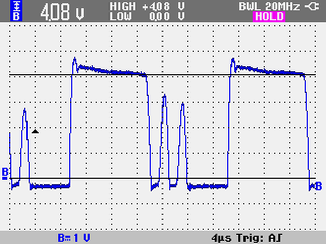
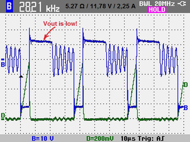
Secondary winding has the same number of turns as aux winding. So Vaux is close to Vsec. As you can see (blue waveform) Vaux = Vsec is approximately 12 V. In my design Rs1 = 50 k, Rs2 = 18 k. So voltage at Vs pin should be 12 * 18 / (50 + 18) = 3.18 V (much less then expected 4.05 V).

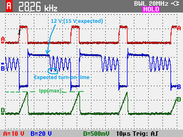
The Vcs signal has a magnitude of 0.75-0.8 V corresponding to Ipp(max). And the output frequency is set to approx. 28 kHz. Note that at lighter load (6.8 Ω) I get higher frequency than at higher load (5.1 Ω).

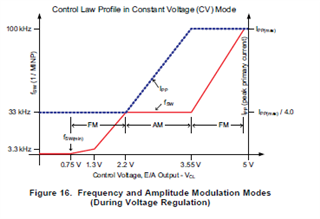
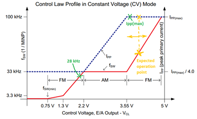
The question is why the frequency is reduced after connecting extra load? As I understand while Vs pin is below regulating level of 4.05 V the output signal should be switched at the first or maybe second valley (Expected turn-on time at blue waveform) and frequency should increase as well as output power. According to control law frequency can NOT be below 33 kHz while current is maximum.

The question is what exactly prevents UCC28711 from increasing the frequency? Or maybe what prevents UCC28711 from switching at the first or second valley providing at least 40 kHz and enough power to keep voltage at 15 V.

  • Hello,

    The transformer magnetizing inductance, peak current and transformer demag time tDmag will set the switching frequency.    

    If your output voltage is too low the transformer turns ratio (Np/Ns) and transformer primary magnetizing inductance (Lp) may not be correct.

    Equation 14 in the data sheet shows how Lp is related to frequency, primary peak current (Ipp).

    Your waveform does show that you are operating at a low frequency  and in DCM.  You are actually operating in the lower FM band.  So the UCC28711 should be controlling the VS pin to 4.06 V at the sample point. 

    You might want to check your VS divider resistors to make sure they are correct as well. 

    Generally  when the output is not regulated the converter will operate in critical conduction.   Your waveforms show deep DCM.  It looks like the controller believes it is observing 4.06V at the sample point.

    Regards,

  • Hello!

    You are actually operating in the lower FM band.

    If we are operating in the lower FM band than the current would be Ipp(max)/4 and CS signal magnitude would be VCST(MIN) = 195 mV. Am I right?

    So the UCC28711 should be controlling the VS pin to 4.06 V at the sample point. 
    It looks like the controller believes it is observing 4.06V at the sample point.

    Lets look at VS pin waveform and again Vaux and drain current (different loads). 


    1. Load 8.65 Ω, Vout = 15.14 V, Iout = 1.75 A, P = 26.5 W

     VS-pin waveform


    2. Load 6.96 Ω, Vout = 15.17 V, Iout = 2.18 A, P = 33.1 W


    3. Load 5.27 Ω, Vout = 11.78 V, Iout = 2.25 A, P = 26.5 W. Vs signal does not even get close to regulating level of 4.06 V.

    Replacing the IC does not solve this problem

  • Hello,

    I am wondering if the issues is your FET is not turning on fast enough which would limit your duty cycle. 

    When VS is below 4.06V at the sample point it should  initiate a gate drive pulse at the first or second valley after tDamg has timed out.  Please note that the UCC28711 will  sample three switching cycles before adjusting the peak current and/or off time to adjust the duty cycle.

    Your last two waveforms show that VS is well before 4.06V and does not turnon the FET until after 5 valleys after tDmag has timed out.  The UCC28711 only had 25 mA of gate drive current available to turn-on a FET.  Refer to the block diagram in section 8.2   If the FET you are using gate capacitance is too large it may cause this issue.  

    Study VS, DRV along with the CS signal to see what is going on an how long it takes to drive the gate through the miller plateau.   If this ends up being the issue it can be resolved by adding an external gate driver with higher gate drive current.  The option is to select a FET with lower gate capacitance.

    Regards,

  • Got it. I'll try to add a gate driver or change the FET. Hope it will work. Thank you for your help.

  • I added the driver (UCC27531), replaced UCC2811 again and found no changes in its behavour. Here is the Gate-Source voltage. MOSFET is STW15N95K5


  • Hello,

    The more I studied these waveforms it looks like the transformer that is used violates the control law and is most likely why your design is having regulation issues.

    The below waveform is operating at 28 kHz the converter should be operating the lower FM band and VCS should be controlled to  VCST(min) = 195 mV.  Your waveforms shows that VCS is controlled to VCST(max) = 780 mV.  I think your issue is that your design is violating control law.  While controlling VCS to VCS(max) the design should be operating above  33 kHz in the upper FM band VCL is between 3.55V and 5V (Control law Diagrams internal voltage amplifier outputs).

    For the UCC28711 work properly when CS is controlled to VCST(max) the design needs to be switching at greater than 33 kHz.  If not the controller will have issues regulating the output as you are observing.

    I would suggest redesigning or selecting a transformer for a maximum switching frequency of greater than 45 kHz. 

    The following link will bring you to an excel design tool that will calculate the primary magnatizing inductance and transformer turns ratio that is required for your design.

    https://www.ti.com/lit/zip/sluc590

    Regards,

  • Thank you for your help! I guess I should redesign the transformer and the PCB. It will take some time. . 

  • The question is what exactly prevents UCC28711 from increasing the frequency?

    The answer is too simple.

    Datasheet says: " DMAGCC is defined as the secondary diode conduction duty cycle during constant-current, CC, operation. It is set internally by the UCC2871x family at 0.425."

    Secondary diode conduction duty cycle (tDM) can not be longer than 0.425 of switching period. Hence the switching frequency can not be higher than 0.425/tDM. While tDM = 15 us, fmax = 28,33 kHz. Exactly like we see it in the first waveform.


  • Hello Oleg,

    You have found the correct reason for the original issue.  The fixed Dmagcc constant is limiting the switching frequency.

    Essentially you were operating in constant current mode (CC) when you tried to increase load from 33W to 44W.  The controller has changed from constant voltage regulation to CC regulation and the 4.05V reference at VS is not involved.   Any further increase in load (decreasing resistance) actually lowers both switching frequency and output power because Iout stays the same, but Vout keeps dropping.

     Since your original target was for 50W, I think maybe you designed it without following the design procedure (or not using the Excel too) and missed the point about the 0.425 Dmagcc factor.  It seems that Mike who tried to help you at first also missed this point, unfortunately, and was trying to fix a problem that wasn't there.  I do agree with a couple parts of his advice however:

    Please begin your design again using the UCC2871x Calculator Tool found here https://www.ti.com/lit/zip/sluc590 which will help obtain the proper parameters for your 50W design. And target a switching frequency higher than 45kHz.  Perhaps with some iteration, you can find a max-load frequency that allows you to use the magnetizing inductance that you already have.  Be sure to allow at least 5% or 10% extra current for the CC target in order to guarantee that your design will always provide at least 50W over the full input voltage range.  And be sure that the core material and size is suitable for that frequency.

    Finally, I think that the apparent instability in frequency that you point out early on in this thread is not instability, but rather is the variations due to the built-in frequency dithering feature.  Very little is said about this feature in the datasheet except for a front-page bullet on "Frequency Jitter..." and a sentence in the 2nd paragraph of Section 8.1 Overview discussing a means to reduce " …EMI peak energy...".  In the UCC2871x family, this dithering (jitter) is relatively aggressive and could appear to be an instability.

    I hope this will help you to achieve your design goals.

    Regards,
    Ulrich