This thread has been locked.

If you have a related question, please click the "Ask a related question" button in the top right corner. The newly created question will be automatically linked to this question.

LM5060-Q1: LM5060Q1MMX/NOPB

Part Number: LM5060-Q1
Other Parts Discussed in Thread: LM5060

HI,

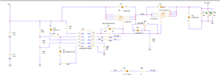
We are working on a automotive solution and have used LM5060 as OVP sw with high side protection.

What I am seeing is as soon as the devices passes UVLO limit the timer capacitor charges to 5.4V and remains there- EN, UVLO, PGD and OVP are all in valid condition.

I tried to reduce the slew rate by adding caps on GATE drive pin (100nF) and adding total 200nF on TIMER pin but the situation remains same as it is.

Can you please let me know what should I do?

Below is snapshot of the circuit- (please note that UVLO and OVP pins are swapped in this symbol here which is corrected in system)

Thanks!

Mandan

  • Hi Mandan,

    Thanks for reaching out to us. Please could you share the following waveforms during startup, means when the device passes through UVLO threshold to understand the issue better.

    1) Voltages across VIN, UVLO, TIMER, and GATE pins

    2) Voltages across VIN, OUT, TIMER pins, and Input current

  • Hi Avishek,

    I am limited to 2 channel scope since I am WFH.

    I am giving you following waveform with the names of images as identifier.

    UVLO B GATE Y

    UVLO B TIMER Y

    VIN B TIMER Y

    VOUT B TIMER Y

    Would request you to please check this priority.

    Please note that when I am isolating the GATE Pin and forcing it with external supply of 5V to mosfet gates rest of circuit works perfectly well. I believe it is the LM5060 which is not turning ON the GATE.

    Thanks

    Mandan 

  • Hi Mandan,

    As we are communicating through private message, I'm closing this thread.