


Hello Team,
according data sheet, revised May 2019:
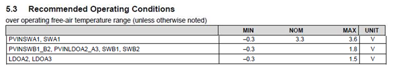
Table in Chapter 5.3, Recommended Operating Conditions:
PVINSWB1_B2, PVI_LDOA2_A3, SWB1, SWB2 shows a maximum voltage of 1.8V,
resp. PVIN_SWA1, SWA1 max 3.6V:
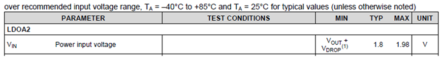
Chapter 5.9 lists LDO2, LDO3 with VIN max. 1.98V (=Pin PVINLDOA2_A3):
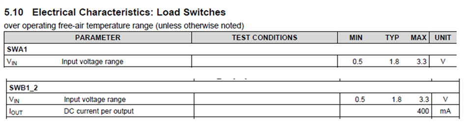
Then in chapter 5.10
SWA1. VIN max 3.3V (= PIn PVINSWA1)
SWB1_2: VIN max 3.3V (= PIN PVINSWB1_B2)
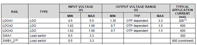
In the Summary Table 6-1:
Input Voltage: 1.98V for LDO2, LDO3
Input Voltage: 3.3V for SWA/SWB
Question:
Which maximum voltages are allowed for PVINSWA1, PVINSWB1_B2; PVINLDOA2_A3, SWB1, SWB2, SWA1, please?
Thanks and Best Regards,
Hans


