


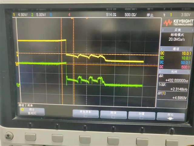
Dear Expert
As for this waveform ,yellow is mosfet Vds waveform ,green is Vgs output waveform . When the MOS is turned off, the waveform is abnormal.
Attached schemetic:
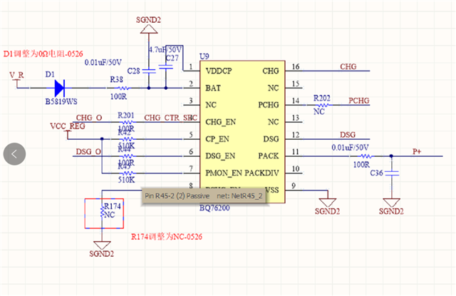
Original question:

BQ76200: Turn OFF time of DSG mosfet is greater than expected
Dear Expert
As for this waveform ,yellow is mosfet Vds waveform ,green is Vgs output waveform . When the MOS is turned off, the waveform is abnormal.
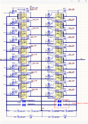
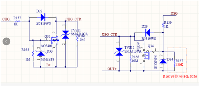
Attached schemetic:
