This thread has been locked.

If you have a related question, please click the "Ask a related question" button in the top right corner. The newly created question will be automatically linked to this question.

TPS63000: Run-time adjustable output via feedback network - not working

Part Number: TPS63000
Other Parts Discussed in Thread: TPS63810, TPS63811, SN74LVC3G07

Hi guys,

TL;DR: I did all the math that seems to work out fine, but I can't get above 3.7v output. My target is up to 6.0v output.

Here's my schematic:

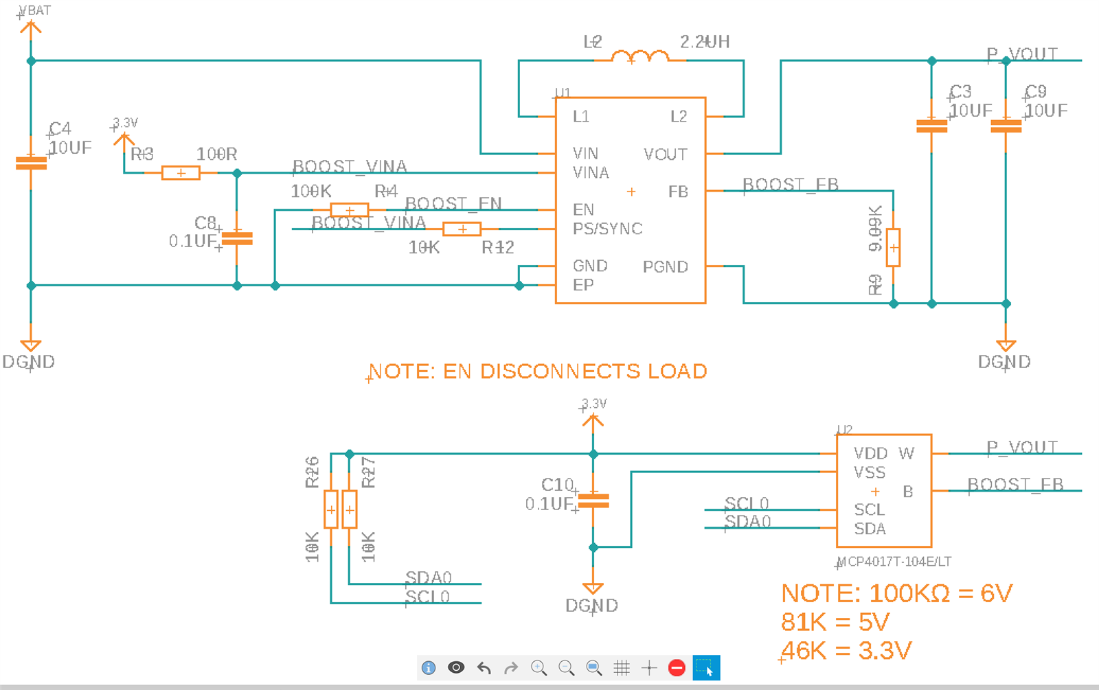
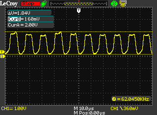
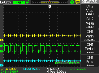
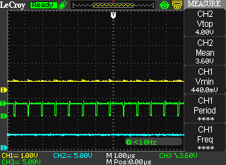
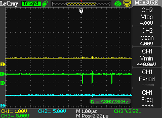
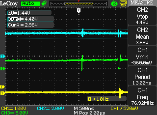
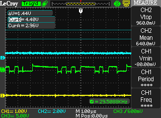
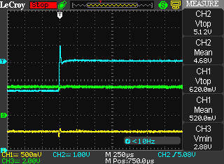
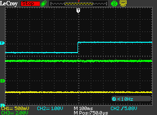
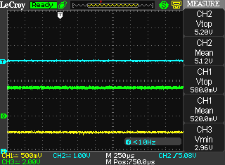
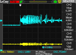
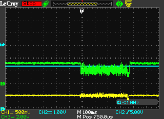
I'm using a digipot in rheostat mode to adjust R1 between 0Ω and 100KΩ. The adjustments work as expected up to ~3.7v when I feed VBAT with 3.2v. It never goes above that however. BOOST_EN is driven by a GPIO at 3.3v elsewhere.

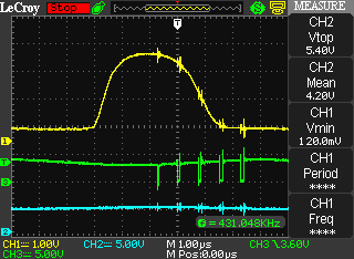
Per the datasheet calculus, this arrangement should provide a boost of up to 6.0v. The inductor I'm using is the Samsung CIGT201610LH2R2MNE (https://www.digikey.com/short/0r02hhb3): 2.2UH, 1.8A, 139mΩ which should satisfy the requirements. I added a 500Ω load and got the same results.

Can you help me understand why this isn't boosting above 3.7v?

  • Hmm, going through the inductor calculus it seems I need an inductor with Isat of 2.5A+, ~3A to satisfy a 20% tolerance.

    Is the inductance value the culprit here? I don't have much space on this PCB!

  • Hi  Nelson,

            I am sorry to tell you that 6V output is not allowed for it may bring a damage to silicon. 5.5V is the max 

            It seems no matter with inductor for the circuit is working with a light load

            I think you can do some check as bellow:

            >>>Features of R1, is it possible a bigger current flows than your set?

            >>>is there a current limit with your source(Vbat)?


  • Hi Tao,

    Good to know for the 5.5v limit, I will limit my software!

    About R1: R1 is an adjustable rheostat, from 0Ω to 100KΩ. I have measured the resistance and it is correct for 3.3v, 5.0v, and 6.0v. R2 is fixed at 9.09KΩ, and measures this value. Current flow through R2 at 5.0v is limited to ~550uA, so current flow through R1 should be less than ~6.1uA.

    Question: Do I need to add an inline resistor between the FB pin and the FB divider network to reduce current flow to the controller?

    About supply current limit: I am powering my circuit with a bench supply limited to 3.3v, 150mA. When I enable the controller with no load, it boosts to 3.7v and draws ~80mA from the supply.

    Question: Do you think the controller is damaged because I tried to set VOUT to 6.0v? I would expect the controller to limit VOUT to 5.5v if that is the maximum.

    Thanks!

  • Hi again, here's what I see on the FB node when I set the network for 5.0v output:

    When I set the network for 2.0v however, I see no activity at all.

    Weird!

  • Hi  Nelson,

          Under normal working conditions, you can consider the FB voltage to be a fixed value close to 0.5V,and the leakage current of the FB PIN is so small that can be ignored. So  the current flow through RI should be same with R2 in normal state

           For your question1: it is no need to add anther resister if R1 has same characteristics as pure resistance

           For your question2: I'm not sure that the chip  damaged due to 6V output, but it is highly probable, could you change another chip and try again?

             The current limit value of the power supply generally refers to the transient current limit, and the measured current value is the effective value within a period of time. So i think you can increase the current limit higher to make sure power supply is ok in your test.

              For your attached waveform, Can you help to capture the waveform of VIN  EN  L1 at the same time based 5V output?


  • I replaced and remounted the TPS63000 as suggested, I'm finding the same results.

    Here are screenshots from my 'scope. CH1: FB, CH2: EN, CH3: L1, CH4: VIN (3.3v).

    Capture #1: VOUT set to 5.0v, drawing ~80mA from VIN. VOUT hovers around 3.7v.

    Capture #2: Curiously, after a few minutes I see this. Please note the 500mV/div change for CH1. VOUT is a steady 500mV!

    Capture #3: EN brought LOW for shutdown. At least that's working lol.


    I admit there may be soldering issues as I mounted the components by hand using hot air and wire solder/solderpaste. I have also checked the pinout and PCB footprint several times, it is correct. I have a TPS63000 EVK on it's way, so I will verify my adjustable FB strategy (digipot) works with a known-good board.

    I'm especially curious about VOUT hovering at 500mV? Could this be a short?

    Thanks, really appreciate your time!

  • Hi Nelson,

            you are welcome and thanks for  your detailed description.

            According to your test results, I strongly suspect that the resistance of R1 is changing during your test. could  you replace R1 with a real resister?

            If R1 is set to 0Ω, output voltage will hover at 500mV too and it is highly probable.


  • Hi Tao,

    I have run some new tests using the TPS63000 EVK. Please note the voltage "settings" are not exact - I am using R2 = 10K and R1 = 100K digipot with Vdd = 3.3v. VIN = 3.3v, 125mA max.

    CH1: FB, CH2: VOUT, CH3: L1.

    Capture #1: VOUT set to "2.5v". VOUT hovers around 2.8v.

    Capture #2: VOUT set to "3.3v". VOUT hovers around 3.6v.

    Capture #3: VOUT set to "3.9v". VOUT hovers around 4.0v. L1 activity is sporadic/random.

    Capture #4: VOUT set to "5.0v". VOUT hovers around 4.2v. L1 activity is sporadic/random, and FB goes crazy, hitting up to 3.0v!


    The MCP4017 digipot datasheet says the FB pin can handle only voltage up to Vdd (3.3v). A friend mentioned that the higher voltage present on FB when the TPS63000 is boosting may be forward-biasing the ESD diodes in the MCP4017, sending higher voltage all over the place.

    What do you think is happening?

    If the MCP4017 cannot be directly connected to the FB network, can you advise a solution to reduce the voltage entering the MCP4017? I see 3 possibilities:

    1. Use an op-amp with 0.5x gain to feed R1 (digipot), where R1 and R2 are both 1/2 their normal value.

    2. Use a voltage divider to reduce VOUT voltage by 1/2 before feeding it into R1, where R1 and R2 are both 1/2 their normal value.

    3. Use MOSFETs or an open-drain buffer to pull current through additional resistors (R2 position) in the FB network.

    What would you recommend for smallest board area?

    Thanks!

  • HI  Anders,

           sorry for calling you wrong for so long.

           I think when Vout is larger than Vdd, logic of  MCP4017 goes wrong and R1 have some strange behaviors. At least, R1 is not a real and stable resister.

           I am sorry that i am unfamiliar with MCP4017 and I don't think I can give you a very good suggestion. could you ask some advice from Microchip?  If your solution is changeable, i think you can use TPS63810 and output voltage is adjustable with I2C. datasheet is attached.

           have a nice day

    Regards

    Tao

           TPS63811 63810.pdf


  • Hi Tao,

    Thank you for your support. It's disappointing to think we cannot find a solution to adjust the FB network using the MCP4017, surely this is possible.

    There is a global shortage of stock for the TPS63811, and it appears the TPS63810 can only output 2 voltage settings which will not work for my application. Can the TPS63810 be programmed to output voltages higher than 3.45v?

    If not, can you please invite someone from Ti that can provide a solution using the MCP4017?

    Thanks

  • HI Anders,

          Good news, I have a discuss with colleagues about your case and a good idea came up. 

          How about replace R1/R2, means MCP4017 connected between FB and GND?  is it possible?  looking forward to your reply

    Regards

    Tao


  • Hi Tao,

    Yes I'm happy to put the digipot in the R2 position. Do you think this will work?

  • Hi Anders,

           For the unstable state of MCP4017 happen when Vout  is larger than Vdd, I think this will work.

           And i think crazy of  FB in your attached Capture #4 is caused by unstable of MCP4017 too, so  this solution is worth trying.

    Regards

    Tao

  • Hi Anders,

          is there any update for your project?

    Regards

    Tao

  • Hi Tao,

    Thanks for your patience. Unfortunately placing the digipot in the R2 position did not resolve the problem:

    CH1: FB, CH2: VOUT, CH3: L1.

    Capture #1: VOUT set near to 5v. VOUT hovers around 4.5v.

    Capture #2: VOUT collapses to around 0.64v, FB apparently shorts to GND.

    I'm replacing the MCP4017 digipot with a Ti SN74LVC3G07, pulling the R2 leg through 3 different R2 values to make 3 different VOUT settings. Do you see any problem with this?

    Thanks!

  • Hi  Anders,

         I'm really sorry for not being able to help you solve the problem in time. to make matters worse, my colleagues and I are not familiar with  SN74LVC3G07 at all, and this may also be the first time we have used this method to adjust the output voltage .

         I will have a discuss about your case with my manager next monday. please wait.

  • Hi  Anders,

           really sorry,  we think we can not give you professional advice about SN74LVC3G07.  sorry again.

  • Hi Tao,

    I'm a little surprised your team can't get any information about a part your company designed and currently manufacturers, but I can tell you this solution works. Using the SN74LVC3G07 to pull the FB network through additional parallel resistance in the "R2" position allows for the output to be adjusted in real time.

    CH1: FB, CH2: VOUT, CH3:VIN.

    Capture #1: VOUT set near to 5v. VOUT overshoots for a few microseconds then holds steady. There are long leads connecting the SN74LVC3G07 to the FB network so I suspect that's why we have such a big transient.

    Capture #1: VOUT set near to 5v. VOUT holds steady. Note 100ms/div timescale.

    Capture #3: VOUT set near to 5v. VOUT steady at 5.12v. Note 250us timescale.

    One problem I encountered was my control system taking a dive once I commanded the FB resistor change, to output 5v. The output would freak out and FB was noisy.

    Adding a probe to VIN shows the input was collapsing during this transition. You can see VIN go down to ~1.0v, and because VIN also feeds the control system, this causes a system reset:

    I added a 100uF capacitor to the input, and the transition smoothed out as seen in the first 'scope image above. Also I found that exceeding max voltage for the FB input will destroy the TPS63000 - after the moments when VOUT would leak through the MCP4107 protection diodes and into FB, the MCP63000 would have to be replaced.

    Hope this helps someone!

  • Hi  Anders,

          Really good news. thanks very much for your great work.

          I want to explain why I can't give you good advice here, i am application engineer form BCS team, Only responsible for the power supply buck-boost solution, so our team  are not familiar with SN74LVC3G07 at all. May be we can connect with other team for help, But I think this kind of communication will be very slow and the product lines on both sides may not be able to give an optimal solution. At this time, our FAE team may be the best choice, because they have an understanding of each product.

         Finally, really appreciate for your work and sorry for i can not give you good advice.

    Regards

    Tao