This thread has been locked.

If you have a related question, please click the "Ask a related question" button in the top right corner. The newly created question will be automatically linked to this question.

TPS61081: TPS61081

Part Number: TPS61081

Hi dear,

I'm using TPS61081DRCR order numbered boost regulator for driving TFT LCD Panel backlight LEDs. I have a trouble. 

TFT LCD screen needs:

Led forward voltage : Min. :7.8V  / Typ. : 9V  /  Max. 10.2V 

Led forward current : IAK : 200mA

The order number of LCD Panel is AMPIRE AM-800480N3TZQW-50H

I need 9V 200mA output from this boost converter.

My schematic is below : 

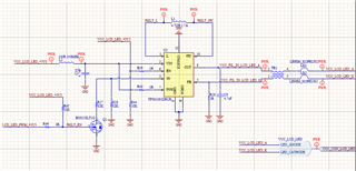
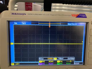
The main problem is that, when I powered my circuit, boost converter didn't give any output only 0V. When I touch the inductor pads, there is no any switching waveform.

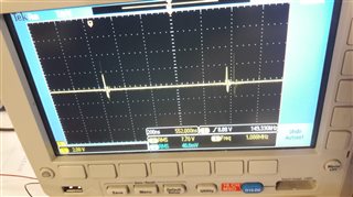
I have detailed my circuit with oscilloscope against voltage spike or etc. on the input pins on TPS61081 but voltage ramps are good.

As an extra information, this circuit is produce +8V3 for LCD backlight for one time an then the circuit didn't work again. (I can not understand.)

When I supply the LCD Anode Cathode pins with external supply as +9V0, LCD is working properly and I can even see some characters at the screen like it must be.

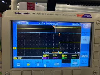
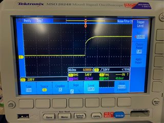
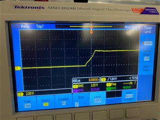
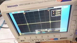
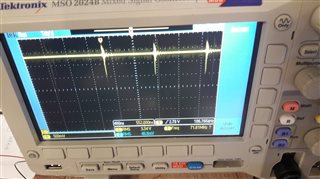
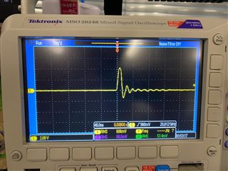
You can find my oscilloscope outputs for ENable signal, +5V0 VIN,  +3V3 supply for LCD (the same as ENABLE signal.), ENABLE signal

BOOST ENABLE signal +3V3 High                                            +5V0 VIN Input voltage ramp                                              +3V3 LCD powre supply ramp

Can the boost converter make protection against the effects that I didn't know it's cause ? The boost converter didn't give any response.  I tried different resistor configurations but these trials didn't affect the result.

  • I'm sorry for the picture, I messed up them.

    +3V3 Enable signal

    +5v0 VIN ramp.

    +3V3 LCD Supply

    The waveforms like burst signals are PWM signals and zoomed version at my first post.

  • Hi Ugur,

    I notice you mentioned the converter is produce +8V3 for LCD backlight for one time an then the circuit didn't work again, since it is current mode, is it possible LCD voltage goes higher and triggers protection?

    1.Could you please measure voltage of IC Vin pin (after input filter) to confirm it not triggers UVLO. When output voltage goes higher, input current increases, voltage drop through source impedance and input filter also increase.

    2.Could you please measure voltage of FB pin and Vout pin (before output filter) when setting LED_PWM constantly high or low? We can confirm output filter does not affect it.

    Or can temporarily remove L2, TR1, LK1 to test board, other parts circuit seems designed okay and should work. 

    Best Regards,

    Eric Yue

  • Hi Eric thanks for your quick reply.

    I realized at my second trials that when I change the TPS61081 IC with new one. The new one can produce +7.3 /8.3 V etc. When I saw this output LCD backlight didn't work properly. I didn't see any character on the screen.

    After short time the output goes 0V again. As if LCD damages the IC. Another ineteresting issue is when TPS generate voltage and supply backlight current. Some noise occurs on the ENABLE +3V3 signals and +5V0 VIN power line. This noise affect +3V3 ENABLE signal voltage, noise decrease this voltage level to +1V6 etc. 

    When I measure noise peaks (noise is affect the +3V3 and +5V0 lines like damped sinusoidal waveform.) I saw that between 2 noise waveform is 780ns. That means 1.2MHz. Disappointed

    Additonall another information is that, when I supply LCD Anode and Cathode pins external +9V0 power supply LCD backlight works properly but backlights current is 420mA. External power supply is constant voltage source. When I use  Constant current like TPS61081, this value decrease to 200mA. Because, LCD datasheet says that Backlight typical +9V0 200mA.

    I will measure your suggestions and then I will reply my result pictures. Thanks you.

    Ugur

  • Hi Ugur,

    This big noise which affects EN and Vin may trigger UVLO and disable or even damage IC if leading to large current. 1.2MHz is just equal to switching frequency, it's interesting how it couples to these two pins. 

    Since external power supply can active LCD at 9V/420mA, maybe you could try to change R27/28 or R26 working at 420mA for TPS61081 to check.

    Best Regards,

    Eric Yue

  • Hi dear Eric,

    I have faced some interesting problems about TPS and my design.

    #1 I said that before you, After a meantime, the TPS61081DRCR IC is damaged becaose of a reason that I don't know . After that, I changed boost IC with new one, adter that the IC started to generate approzimately +7.8V and then I connect my LCD and there is no any lightning on the screeen.

    After my a few trials, the IC started to generate only 1.5V and this state didn't change anymore. (I think IC is damaged ?)

    First issue is that.

    #2 As second, When IC boost +5V0 input to +7.8V output, there is some anormal waveforms at +3V3 pull up line for enable pin and +5V0 main VIN pin. You can see from the pictures these power lines.

    +5V0 VIN


    +5V0 VIN

    +3V3 ENABLE

    +3V3 ENABLE

    #3 When IC generate this +7V7 after short time the output gose to +1.5V-2V0 and then this output voltage didn't change anymore.(IC is damaged. I think.)

  • Hi Ugur,

    #1 Whether the output is still 1.5V, after LCD is disconnected? And you can test input/output resistor to conform whether IC is damaged. If damaged, I notice when powering 420mA, LCD can work, maybe large load current damaged the chip and you can try to change R27/28 or R26 working at 420mA like I suggested before.

    #2 From the waveforms of 5V0 VIN, I think the voltage is about 8V, is it the output voltage? What is Vin at this point? You can check VCC_LCD_LED3V3 because EN signal is input signal.

    #3 Similar to #1, you can try to disconnect LCD and change load set current to 420mA.

    Can you provide datasheet of your LCD? I cannot find it on Website. I can try to imitate your test in bench through constant voltage source series resistor to imitate LCD characteristics from its V-I characteristics. BTW you can also try measurements and methods I mentioned before to check.

    Best Regards,

    Eric Yue

  • Hi Eric, 

    #1I think I resolve the problem. I changed inductor with different higher current type and then the boost converter produce iTs output voltage current etc. properly.

    #2 However, I could'nt not change screen brightness by changing R1,R2 and RSET resistor values. Finally, I didn't populate BSS138 NMOS PWM dimming transistor. After that brightness is now very good. PWM Duty cycle is affect the brightness level ?

    #3 Finally, I connected 82K resistor to SS pin and 10R rset resistor. According to these components, LED current calculation must be (82K*5uA)/10R=40mA but when I have detailed my power supply, LEDs are supplied with approximately150mA The formulas and practice doens't comply. What is the reason of that ?

  • #4 An additoonal question, I didn't understand this ICs working principle, I couldn't understand How pWM signal effect SS pin and this feature effect brightness or etc. Could you please make some explain how this IC is working ? Thanks you. Or you can send me detailed any document.

  • Hi Ugur,

    #1 What is inductor current now? If load current is 200mA, 1.7A inductor seems will not saturate.

    #2 PWM duty cycle will change effective resistance of SS pin, so FB voltage will change.

    #3 From datasheet, it should be 40mA, could you please measure FB pin voltage to confirm whether it is 82K*5uA? Is there any possible current path except FB pin?

    #4 Sorry, I am not familiar with LCD, from TPS perspective, PWM will effect resistance of SS pin and FB voltage is changed. For fixed RSET resistor, current through RSET which is equal to LCD is changed. Then I think changed current will effect LCD brightness. May I confirm LCD current will change brightness? Please let me know if you have a different thinking.

    Best Regards,

    Eric Yue