A related question is a question created from another question. When the related question is created, it will be automatically linked to the original question.
If you have a related question, please click the "Ask a related question" button in the top right corner. The newly created question will be automatically linked to this question.
Are you looking for a constant current load from a 2V source capable of sinking 2A of current?
Can you afford a bias voltage to operate this current sink from?
Can this be a linear (non-switching) load or do you need as switch-mode constant current load that will recover the sink energy back to the bias supply?
It sounds like you need an active load. One solution that I have seen is to use a current sense resistor and an amplifier to drive the gate of a FET. You are essentually designing a closed loop system that biases the gate of the FET such that it sinks a constant current. Please consider using Texas Instruments amplifiers for this function. Our family of INAxxx current sense amplifiers might be useful.
This current sink is for biasing the power supply taps of a sensor, and those power supply taps are switching ( Transient time is 30ms) between current source( +15V and 2A this is easy to implement by TI power chip) and current sink ( 2A and DC +2V output).
At beginning I want to use MOSFET and resistor to realize this current sink
But sensor guys don’t want any resistance on current sink path since it will generate the noise, but I told them it is impossible without resistance on current sink path.
But right now they can’t provide me the resistance limitation.
Are you looking for a constant current load from a 2V source capable of sinking 2A of current?
Can you afford a bias voltage to operate this current sink from?
Can this be a linear (non-switching) load or do you need as switch-mode constant current load that will recover the sink energy back to the bias supply?
I am think I am looking for 2V source capable of sinking 2A of current for now.
I think I can afford a bias voltage to operate this current sink.
For the third question, please check my application explanation below.
Sensor guy asked me about this current sink again, so sad!!!
If I am understanding your requirement right, you would like a 2-state non-isolated DC/DC Converter capable of sourcing current at a 15V output and sinking current at a 2V output?
If that is correct, there are several ways to do this. One of the easiest ways would be to use the TPS40056 controller with a 10:1 feedback divider. The TPS40056 controller uses an external reference input, allowing you to set the EA+ pin voltage to 1.5V for a 15V ouptut and 0.2V for a 2V ouptut. Controlling the slew-rate of the EA+ pin would allow you to slew between the two states at a controlled rate.
The fully-synchronous architecture of the TPS40056's power stage allows it to provide a regulated output voltage while both Sourcing Current and Sinking Current.
Note howevre, when a switch mode power supply sinks current, the energy is boosted back to the input voltage so the source MUST be able to sink current or additional loads that share the same source voltage must sink more energy than is boosted back from the active load (sinking power supply) to prevent the input voltage from increasing and causing an over-voltage condition.
Do you know if the sensor needs a fixed voltage (and source or sink what ever current the sensor requires) or a fixed current (generating the voltage the load requires) ?
The sensor needs fixed +2V when it is in current sink mode.
I am thinking how about use a liner regulator as current sink and use TPS5450 for +15V +2A current source supply; two load switches will make the connections with sensor.
The reason why I choice above idea is there are lot of power supply taps need this current sink mode and I am afraid the power consumption is over the limit.
If it is possible please let me know other current sink ideas.
If you're just looking for a circuit to sink current to maintain a 2V input voltage, you can build such a circuit with an Op-Amp and a MOSFET.
The Op-Amp becomes an error amplifier, comparing the ouptut voltage to a reference voltage, and driving the GATE of the MOSFET to sink current from the output voltage.
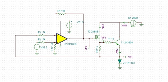
I think you make need to check that circuit, there doesn't appear to be any feedback path from the output voltage or current.
Also, we need to understand if you need a Current regulator or Voltage Regulator. Your earlier message seemed to indicate that you needed a voltage regulator.
The above circuit's op-amp is driving VF1 (voltage drop across D1) to be equal to VS2 (which looks like 5V) but with a limited gain stage (R4 / R3 = 1)
Have you simulated this circuit with a resistive source at the ouptut voltage - say a 10ohm pull-up to 22V (which should draw 2A if the ouptut voltage is driven to 2V) ?
So sorry for the unclear information I provided to you.
Yes, I only need a voltage regulator with +2V output.
I configured that op amp as difference amplifier, the function of this op amp is to fine tune the P mosfet to let it turn on further or lower based on the forward voltage of diode( this diode can carry 200mA with 700mV, I don't have diode model which can carry 2A at 2.1V forward voltage).
Yes, you are right that reference voltage should be 700mV.
Based on my previous experience with TINA the difference amplifier can’t work properly and I have asked technical support from TI regarding to difference amplifier, they can’t figure it out.
I have simulated this circuit without that op amp; the rest of circuit can work.
Let's look at the FET. The source is connected to the base of T1, whos emitter is at VF1, which presumably we want at 0.7V, so we'll estimate the base voltage is about 1.4V. This would cause the Gate-Source voltage of T2 to be - 1.4V.
If the diode voltage (Vf) is low, (0.6V) the Op-Amp's ouptut increases (0.1) increasing the Gate-Source voltage on the P-channel MOSFET (less negative), reducing the current into the BJT's base, decreasing current, decreasing Vf. This increases the ouptut voltage, further decreasing the Gate-source voltage on the P-channel MOSFET until Vf = 0, the gate of the P-channel FET is +0.7V, holding the MOSFET in the OFF state.
I don't think this circuit will work to regulate a 2V output voltage.