


Hi ,
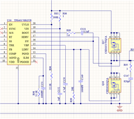
In what condition a "shoot-through" scenario could happen on this configuration that could damage either the high drive or low drive FET?
Thank you.
Jojo
Hi ,
In what condition a "shoot-through" scenario could happen on this configuration that could damage either the high drive or low drive FET?
Thank you.
Jojo

