This thread has been locked.

If you have a related question, please click the "Ask a related question" button in the top right corner. The newly created question will be automatically linked to this question.

TPS546D24: Power management forum

Part Number: TPS546D24

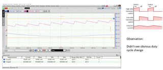
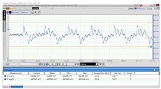
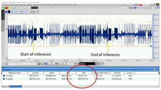
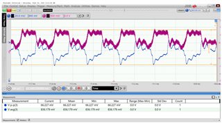
We designed this part TPS546D24 in our PCIe card outptut ripple is very high - 0.8V@8A load the ripple is about Vp-p= 90mV. Ripple current is +/-3A. Due to this we cannot run the processor at higher speed & higher load. We need you to verify that we have the design the TPS546D24 correctly for least ripple.

Vout = 0.8V

I out = 20A max

I out trans = 10A max

Fsw = we have selected 900KHz but we can change this for least ripple.

C out = ~ 2000uF

Inductor  = 0.3uH with 32A current & max DCR=1.1mOhms -- ASPIAIG-F1040-R30M-T

Regards,

Farooq (408-482-2315)

  • TPS546D24 Scheamtics is attached

    Look at teh switchign current thru inductor the then ON/OFF time does not change with load current.

     TPS546D24_SCH_082120-edits.pdf

  •  

    Ideally, On-time should not change with load current.  Typically, on-time changes with load current to compensate for increased power losses.  If the efficiency is good, and consistent over load, the less you'll see the on-time change over load.

    You had 3 posts on this same topic, I deleted one of them, but this one has  additional files linked into it, so I will copy my response to the other thread here and delete it to consolidate them into a single thread.

  •  

    I am sorry to hear that you are having issues.

    Can you tell me, is the output ripple that you are seeing at the 900kHz switching frequency, or is it at a lower switching frequency?

    Is the ripple generally triangular / sinusoidal in nature, or or is it pulses at the switching frequency?

    Can you share a picture of the output ripple?

    90mV output ripple seems really high, especially for 2000uF output capacitance and 3A of ripple.  Typically, output ripple, at least at the switching frequency, is a result of the inductor ripple current and the impedance of the output capacitors.  If you are seeing 90mV of triangular or sinusoidal, then I think you need to review your output capacitors and layout for sources of parasitic resistance.

    If the 90mV output ripple is square-wave pulses in time with the switching node, you are either looking at a measurement technique artifact, like inductive coupling in to the oscilloscope probe ground lead, or high parasitic inductance in the output capacitance.

    If the 90mV output ripple is at a lower frequency, below the 900kHz switching frequency, we may have to look at the compensation.

    First, can you confirm if you are using the TPS546D24 or TPS546D24A?   The D24 and D24A are difference devices that use different programming resistors to obtain the same programmable settings.

    If you are using the TPS546D24, did you select the MSEL1, MSEL2, VSEL and ADRSEL programming resistors based on a D24 design tool or base don a D24A design tool?  They are not the same, and the TPS546D24 will not work correctly if the resistors are selected using the D24A design tools.

  •  

    A few things that I noticed about your schematic:

    1) You do not have separate nets for AGND and PGND.  While AGND and PGND need to be connected at the layout under the IC between the AGND pin pad and the exposed pad (EP) providing separate nets to limit switching ground noise between sensitive components and their ground return is recommended.

    2) VOUT is not connected on the schematic page with the output voltage going to MON_VDD_CORE_P on page 18 and the sense coming back from VDD_CORE_R on page 7.  If there is a long routing distance from VOUT local to the converter and VOUT sensed  remotely at the load, that can introduce parasitic inductance, which can react with local bypass capacitance at the load to add an additional L-C filter, and associated phase lag, to the loop.  If we are seeing a low-frequency oscillation in the output voltage, that could be the source.

    3) There is no ceramic output capacitance provided on the schematic, just 5x 220uF 4V electrolytic capacitors, which could also be the source of the high ripple.

    I would recommend considering moving this design to the TPS546D24A, which is a pin to pin and layout compatible deice with updated Pin Programming options.

    If you can share the details of the 90mV output ripple, we can likely find the source of this issue.

  • Hi Peter:

    thanks for your response.

    First of all -- we used TPS546D24 programming resistors -- -not the D24A version. THat was issue when we first did the bring up of the proto boards.

    We are using the 900KHz after looking at 325, 550 and 650 and even 1100 - 900KHz gave lowest ripple with stability with static loads. 1100 was not stable some of the times.

    See the ripple picture attached. One with full capture, second is zoomed in and third is with current thru inductor.

    We have oscillation at ~30KHz and ~10KHz

    We do have more capacitors detaisl of number of caps is below--- only the 220uF are "TMCMA0G227MTRF" tant cap rest are all ceramics.

    1. PGND and AGND are not separate. Is that critical issue?

    2. We have an ADC monitoring the out pout voltage on page#18. The sense coming back from page#7 is coming from Processor chip itself. Trace length would be couple of inches. BUt connected this to Vout locally but the ripple was still the same. 

    3. We have the follwoing caps on the VDD_CORE_0.8 rail

    22x 0.1uF, 52x 1uF, 5x 4.7uF, 4x 10uF, 4x 22uF, 1x 47uF, 3x220uF, 11x100uF

    5x 220uF -- these five are in addition to above & placed close to TPS546D24.Only the 220uF are Tant cap rest are ceramics.

  • I can see two ripple components in the output.  One with about a 25us period and one with a 150us period.

    Is this taken under a steadystate, or is the output being pulsed with a 150us period dynamic load?

    The 40kH looks like it could be a layout induced resonance.  Is the compensation Pin programmed or custom programmed via PMBus?

  • HI Peter:

    the processor has multiple cores which turn on/off depending on what data they are proocessing.

    transient curent is about +/-4A on top of 7A average - in the picture shared.

    these reading are taken with pin prgrammed configuration

  •  

    Reviewing your pin programming options, it looks like the Compensation Code is 3, which sets the current loop gain to 2x and the voltage loop gain to 2x, which is very low for your 300nH inductor at 900kHz and the large amount of output capacitance you have.

    I think Compensation Code 29 would be a better option, rather than Code 3.

    If you want to try Code 29 our without changing the resistors, you can use the FUSION software to program COMPENSATION_CONFIG.  You will need to either:

    1) Disable the output voltage while programming the COMPENSATION_CONFIG value (it will not update while the output is enabled)

    2) Write COMPENSATION_CONFIG and update the PIN_DETECT_OVERRIDE value to load COMPENSATION_CONFIG from NVM instead of pin-strap, then cycle the AVIN power.

    The hex value is: 13 40 42 1C 84h

    The breakdown is:

    GMI 200uS, RVI 35kOhms, CZI Multiplier 160, CZI 106pF, CPI 6.4pF

    GMV 50uS, RVV 80kOhms, CZV 250pF, CPV 6.25pF

    That will offer higher current loop bandwidth and higher voltage loop bandwidth.

    If that woks for you, the MSEL1 resistors would be:

    71.5kOhms to AGND, and 28.7k to BP1V5

  • Hi Peter:

    We did compensation changes with 300nH and also 200nH and 150nH inductors - see the readings below.

    From 93.4mV p-p ripple with Comp code 3, we have it down to 44.5mV p-p using 150nH with Comp code 20. We want to use the resistors to set the compensation as the boards are in pre-production stage.

    Can you confirm the values of Comp code 20 ? 

    Inductor Value (nH)

    300

    300

    300

    300

    300

    300

    300

    200

    200

    150

    150

    iLOOP Gain/vLOOP Gain

    2/2

    7.5/7

    7/4

    10/4

    10/5

    10/6

    10/10

    10/6

    7/5

    7/5

    5/8

    VDD Droop P-P (mV)

    93.9

    97.8

    62.7

    57.9

    53.8

    65.4

    153.2

    47.9

    44.1

    44.2

    44.5

  • HI Peter:

    I meant - confirm the resistors values for the Comp code 20?

  •  

    For the TPS546D24, the MSEL1 to AGND resistor sets the Compensation Code and the divider ratio sets the switching frequency.  The Compensation Code is always equal to the resistor to ground resistance and 900kHz is divider code 5.

    For Code 20, 900kHz that's 

    30.1kOhms to GND and 12.1k to BP1V5

  • thanks Peter:

    Let me validate the ripple on multiple boards with these resistors then i shall come back in few days.

  • I can give you the PMBus programming values if that is faster for you to experiment with.

  • HI Peter:

    I worked using different values for Comp Code and measured the ripple, on multiple cards.

    We changed the bulk caps to be lower ESR versions which also helped. Now the ripple is looking much better.

    Now i have final few questions for you;

    1. The resistors values for MSEL1 for 0.8V with 900KHz for divider code 29 (or iLoop/vLoop = 7/4)?

    2. Should the inductor value be closer to Maximum recommended inductor value (inductor ripple10% of full load) OR close to Miniimum recommended inductor value (inductor ripple40% of full load) - for least ripple on the voltage rail?? What is best inductor value for largest margin in load current?

    3. Other that these Comp Code (1-29) - other compensation values which are configurable thru I2C - why are these not in the included in table in the "Compensation_Calculator_PG3.xls"? Are those compensation values "VALID" for use in production released products? How can i confirm the compensation code (above 29) that looks better to me ripple-wise is a "VALID" selection?

    4. Can/How to calculate the resistors values for Comp code higher than 29???

    Regards,

    Farooq 

  •  

    1) What are the resistor values for MSEL1 with 900kHz for divider code 29?

    This is Pin to Ground code 29 and Rdiv 5, which is 71.5kΩ to AGND and 28.7kΩ to BP1V5

    2) What inductor value will produce the lowest ripple?  What inductor value will produce the greater load current margin?

    The highest inductor value (closest to 10% ripple) will generally produce the lowest output ripple, especially cycle by cycle output ripple rather than transient response ripple.

    Lower inductor values (closest to 40% ripple) will generally produce the lowest transient ripple in response to a load change and the greatest margin for maximum load current due to lower DCR and higher saturation current.

    3) Why are programming values not in the 1-29 range no listed in the valid compensation range?

    The TPS546D24 has 35-bits of programmable compensation providing 34 billion possible compensation values.  It is simply not possible to provide an evaluation of all of them.  the Excel spread-sheet provides an evaluation of the 29 available pin-strapped values and guidance to generating a valid custom programmed value which can be programmed via PMBus.

    4) How to calculate resistor values to program Compensation Codes greater than 29?

    Compensation Codes 1-29 can be programmed via Pin Programming, other values of COMPENSATION_CONFIG can only be programmed through PMBus.

  • Hi Peter:

    thanks for your reply;

    in #3 --  How do i know the Comp code that gives me better ripple wavefrom -- is "valid" Comp code as there are some Comp code which are RED in color, as invalid??

    Regards,

    Farooq

  • Hi Peter;

    Clearifying my question--

    in #3 --  How do i know the Comp code (selected thru PMBus) that gives me better ripple wavefrom -- is "valid" Comp code, as there are some Comp code (pin prgramming) which are RED in color or invalid?? Some of these PMBus selectable Comp codes are Valid & some are not.

    Regards,

    Farooq

  •  

    All 1-29 codes are "valid" in that they are pin programmable and will result in valid data.

    The Red and Green guidance provided in the COMPENSATION_CONFIG design tool is highlighting pin programmable compensation codes that provide the current and voltage loop bandwidths that are equal to or less than the targets provided with the power-stage inductor and capacitors entered into the tool, and provide at least the same ILOOP to VLOOP bandwidth ratio.

    If you are using custom PMBus programming rather than pin-strap programming, then you'll enter the compensation values in the section below that in the design tool, and warnings will highlight in RED if the design violates one of the design criteria.

    For example, on a design running at 900kHz, if you enter a Fsw/ILOOP ratio target of 4, and a Fsw/VLOOP ratio target of 8  the tool will highlight pin programmable compensation codes that provide a current limit bandwidth of upto 225kHz (900/4) and maintain at least 2:1 (8/4) ratio between the ILOOP bandwidth and the VLOOP bandwidth.

    ILOOP gains that push the current loop bandwidth ovee 225kHz or VLOOP gains that push the VLOOP over 1/2 the ILOOP bandwidth with the selected ILOOP gain on that line, will be highlighted RED.

  • Thanks Peter for calrifying the points.

    What does it mean (in terms of regulator performance, ripple etc) if changing the Fsw / Fcov from 10 to 9? By default its 10 with a recomended range of 8-12.

    Regards,

    Farooq

  • Hi Faroop,

    Peter and US team is on holiday. Please wait and hope he can respond to you on Tuesday US time~

    Thanks,

    Lishuang

  •  

    The Ratio of the target Voltage Loop Cross-Over (Vco) to the Switching Frequency (Fsw)  helps the tool set the target voltage loop bandwidth.

    The higher the target bandwidth, the quicker the voltage loop can respond and change the current loop's target current in response to a change in the output voltage.  That will increase the converter's ability to respond to system dynamics such as changing in the load current to maintain a constant output voltage.  In a typical load-transient test, higher bandwidth will result in less drop or rise in VOUT during a load change.

    Reducing the target from Fsw / 10 to Fsw / 9 increases the loop bandwidth about 10%, but this also makes the loop more susceptible to unmodeled parasitics such as ESL, power path inductance and resistance, which degrades the gain and phase margin of the loop.