This thread has been locked.

If you have a related question, please click the "Ask a related question" button in the top right corner. The newly created question will be automatically linked to this question.

LM25117EVAL: Mosfet gate resistor design

Part Number: LM25117EVAL
Other Parts Discussed in Thread: LM25117

Hi, I’m starting using your LM25117 buck controller.
I need to understand how design the resistors in series with the power mosfets.

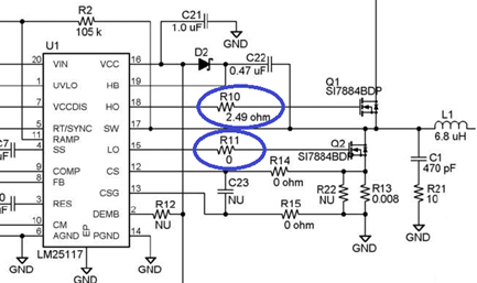
In your demboard «AN-2112 LM25117 Evaluation Board» the schematic is the following

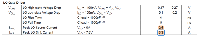
The driver currents in LM25117 datasheet are

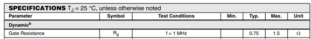
The internal resistance of the mosfet SI7884BDP in its datasheet is

The low side mosfet is considered ( Rgate_external = 0 Ohm).

In my opinion, the driver peak current  is 

I_driver_peak = Vcc / (Rgate_internal + Rgate_external ) = 7,6 V /  (0,75 Ohm  +  0 Ohm) = 10,1 A

That current is very high compared with datasheet maximum driver current.

If  R_gate_external = 2,7 Ohm is used, the peak current is

I_driver_peak = Vcc / (Rgate_interna + R_gate_external) = 7,6 V/ (0.75 Ohm + 2,7 Ohm) = 2,2 A

In my opinion R_gate_external = 2.7 Ohm is ok.

My questions are:
1) There is something wrong in the demoboard low side mosfet design ?
2) My design method is correct ?

Take into account that the buck converter is used in a very important PCB for my company, so the most important thing is the reliability of the circuit.

p.s.  I think that in the demoboard, the high side mosfet total gate resistance is higher than the low side mosfet one to reduce the voltage ringing on the switching node, it is correct ?


Thanks.

  • Hi Francesco,

    The peak driver instantaneous current occurs during the charging of the gate capacitance, not in steady state as suggested by your calculation above (that uses the DC resistance of the driver).

    In general, a gate resistor is not required on the low-side FET. In many cases, it is actually detrimental as a fast dv/dt on SW can couple current through Cdg into the gate, possibly causing unwanted turn-on.

    A gate resistor on the high-side FET slows switching, albeit with a certain switching loss penalty.

    Regards,

    Tim

  • Thanks for your answer, I try to explain my idea in another way.

    In my opinion, before the low side mosfet is turned on V_gs = 0 V, so the C_gs is no charged.

    When the low side mosfet is turned on, there is a very short current glitch (on the driver output) with the current level that I found with my formula.
    This happen because C_gs is empty, so the current glitch is similar to the initial current in a RC filter with C initially discharged. (the mosfet has its particular turn on behaviour, so after the initial glitch it is completely different from an RC filter).

    Maybe my error is to consider the current expressed in the  LM25117 datasheet as the maximum current allowed during the glitch above indicate, and that if the current glitch exceed that value the IC can be damaged

    Maybe in reality the currents in the datasheet are the maximum currents that the driver can provide and they are internally limited (like a current limiter) so it is impossible for the IC to provide currents greater also for a very short time.

    So in that case you can connect any mosfet (also with big size, high gate capacitance  and zero internal gate resistance)  to the driver without external gate resistance, because the driver is protected from overcurrent.

    There is no possibility to damage the IC even if  the initial current glitch (obtained from the formula)  at the mosfet turn on is greater than the datasheet current value because they are internally limited.

    In that case the maximum IC driver current in the datasheet together with the gate capacitance value are used to know the turn on speed.
    And the use of a driver that can provide a greater maximum current is helpful to increase the mosfet turn on speed, but not for avoid IC damage.

    That idea is correct ?

  • Hi Francesco, there is no risk of IC damage related to current. However, the driver inherently has some dynamic source and sink impedance during turn-on and turn-off that adds to the internal gate resistance of the FET and the externally added gate resistance.

    Regards,

    Tim