This thread has been locked.

If you have a related question, please click the "Ask a related question" button in the top right corner. The newly created question will be automatically linked to this question.

TPS6594-Q1: PTPS65941212RWERQ1 BUCK OUTPUT ISSUE

Part Number: TPS6594-Q1
Other Parts Discussed in Thread: TDA4VM, MSP432E401Y, TPS22965

Hi TI Support Team

We use LEOA (TPS65941212)+LEOB(TPS65941111) for customer board for TDA4VM design. 

One issue finding when we do the power cycle test:  (Battery Power on  / Battery Power off ......) about every 2 second one cycle. 

Sometimes the LEOA buck can not ouput VDD_CPU_AVS (0V8) voltage, The issue happen frequency about 1 /10 times. 

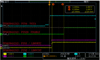
We confirm the VCCA / ENABLE / LDORTC/ LDOINT output voltage correct.  

1. Do you know in any condition the LEOA buck can not output correct voltage?  

2. How to check which error detection to stop the buck power-up from LEOA?

3. Do you have timing requirement for VCCA to Enable ?  Currently we have 10ms from VCCA to Enable. 

4. Any suggestion for this issue. 

Customer board test result:

Thanks

Yutai

  • Hello,

    Can you confirm which devices you are using?   In the title you mention the PTPS65941212.  Please read out register addresses 0x1, 0x2, and 0x3 from I2C addresses 0x48 (PTPS65941212) and 0x4C (PTPS65941111).  Is BUCK123 the only rail not turning on or do all rails and GPIOs fail to turn on?

    (1) Depending upon the NVM version being used, it is likely that the residual voltage check is failing.  During the battery cycle testing is the enable pin low pulled low before the VSYS is removed?  

    (2) The PMIC registers 0x5A-0x6C, contain information about which faults occurred.   Please read out these register addresses for both 0x48 and 0x4C.  Note, that the VIO voltage is supplied by a load switch which will also be turned off if BUCK1-3 is also off.  The VIO voltage will need to be supplied externally in order for the I2C interface to work correctly.

    (3) There is no timing requirement other than the voltage on the enable pin cannot be greater than VCCA.

    (4) How much time is between the power off to power on?  The power down sequence takes about 16ms.  Does the power up start before the power down is complete?  What is the residual voltage on rails when the power up is started?

    Thanks and Regards,

    Chris

  • Hi Chris

    I will update the register value to you later.

    Thanks

    Yutai

  • Hi Chris

    We are waiting the "MSP432E401Y" EVM for PMIC GUI to read TPS65941x register. After when I got it, I will do the test and share those register value to you later. 

    More query about the Residual voltage check from TPS65941212 and TPS65941111. 

    As TPS65941x check Residual-Voltage on the output rail when it drop below 150mV before next Power-Up again and NVM default setting to enable residual voltage checking feature. 

    From Figure 10-39  power transition states of the FSM engine

    Question:

    1. During the battery cycle testing, if TPS65941x LDO/BUCK have residual voltage, then PMIC detect this error.

       So it can not output any voltage for BUCK1..5 and LDO1..4 except LDOINT and LDORTC.  Is it correct ?

    2. Do you know if TPS65941x will re-try the residual voltage check after first fail/ error. How about the timeout and how many time re-check?

    3. From NO SUPPLY => INIT, the only condition is VCCA>VCCA_UV ? 

       Do we need enable pin pull high & VCCA>VCCA_UV for station transfer  ?

    4. Currently we find the residual voltage > 150mV for 3V3 in TPS65941111 FB_B3/Pin49 and FB_B4 / Pin 50. 

        I don't know if it the root cause for PMIC output issue in our battery cycle test. 

        If Yes, Do you have any suggestion to fix this issue and we already use TPS22965 load switch, It have the discharge resistor inside.

    Thanks

    Yutai

  • Hello,

        This will depend upon the NVM revision that you are testing.  If you have the latest revision, then the residual voltage check is only enabled and checked in the BOOT_BIST.  If you have an earlier version, then the residual voltage check can also take place during the power down sequence.

        Again, depending upon the NVM revision the number of retries could be 1 or 15. 

        Yes.  The enable PIN must go high to go to the active state and turn on the regulators.

        The TPS65941111 does not use the FB_B3 and FB_B4 pins as the default configuration.  If these monitors are being turned on by the software then they must also be turned off appropriately.  Please provide more details on how FB_B3 and FB_B4 are used.

    Thanks and Regards,

    Chris

  • Hi Chris

    Thanks for your support. After we are remove the peripheral's power source. Then we can get the correct residual voltage to meet TPS65941x requirement. 

    So we can PASS the battery cycle test. 

    Thanks

    Yutai