This thread has been locked.

If you have a related question, please click the "Ask a related question" button in the top right corner. The newly created question will be automatically linked to this question.

UCC28061:Channel B single phase operation in light-load condition

Part Number: UCC28061
Other Parts Discussed in Thread: UCC28064,

The operation in the no-load state immediately after startup is always GDB (channel B) only.
Is this a normal operation in light-load?
I could not check this mode in the data sheet.

Phase switching is controlled by external control to the PHB terminal, and the PHB terminal is set to Hi for interleaving at startup.

If the PHB terminal remains Hi even after the output voltage stabilizes, is there a possibility that GDB (channel B) single operation will occur?

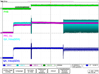
Is there a mode in which GDB (channel B) standalone operation occurs other than the question content?
再試行しています...
再試行しています...
  • Hello user,

    during the start up, Phase B will have pulse output even that PHB is connected to VREF with high threshold. this is normal.

    after start up, if the PHB is connected with Comp, then it is possible that comp pin voltage is less than the threshold of outputting pulses, at this condition, you have a chance with GDA no pulses GDB outputting pulses. if the PHB is connected with Vref, GDB should not output any pulse.

  • After startup, the PHB is not connected to the COMP, but 5V is applied to the PHB.

    Is it possible that only GDB will always be turned on in this situation?

    "If the PHB is connected with Vref, GDB should not output any pulse."

    I don't understand the meaning of this sentence.


    I haven't connected the VREF terminal to any other pin.

  • if the PHB is connected to 5v, when comp pin below 5V, GDB should keep off  after start up.

    is it possible that customer mis-match the channel A and channel B?

    I suggest you can use a new samples for the debug, and double confirm whether ZCDB /GDB for the same channel and zcda/gdb for the other channel.

  • I checked the terminal connections, but there was no mismatch the channels A and B.

    After booting, V (COMP) = 2.5V and V (PHB) = 5V, so GDB should stop, but it is a single operation.


    Is it strange that V (COMP) = 2.5V even though there is no load?

  • Hi user,

    sorry about my mistake to confuse the PHB function between UCC28064 and UCC28061.

    For UCC28061,  If the PHB is connected to 5V, because the two phase mode threshold is 1V, once the PHB is higher than this threshold, PHB will enable. there is no relationship between Comp and PHB.

    according to your question, whether only GDB output pulses at no load or very light load condition?

    once we add a little more load, the GDA will output the pulse?

    if yes, it is a normal phenomenon.

    that is because at no load condition if the Comp Voltage is lower than 222mV, then both GDA and GDB will stop the pulse. And at this condition,

    GDB output some pulses to allow the regulated voltage to be stable, and in the Phase A On time Control diagram, still phase A is stopped because it still do not achieve Comp pin higher than 222mV requirement.

    hope this is clear.

  • As pointed out, only the GDB output is pulsed with no or very light load, and with a little load, the GDA outputs a pulse.

    Is the "regulated voltage" the reference voltage inside the IC?

  • Hi Mukaide,

    if you slightly increase the load, Does GDA still only output one pulse?

    I think at no load or very light load for GDA it maybe only one pulse, the pulse number depends on how long the Comp pin voltage over the 222mV threshold.

    once the Comp pin voltage goes higher than 222mV when you increase the load, GDA should not only output one pulse.

    the requlated voltage here is the PFC output voltage(PFC bus cap voltage)

  • As explained, when the COMP voltage exceeded 222 mV, both GDA and GDB output pulses.


    [that is because at no load condition if the Comp Voltage is lower than 222mV, then both GDA and GDB will stop the pulse. And at this condition,

    GDB output some pulses to allow the regulated voltage to be stable, and in the Phase A On time Control diagram, still phase A is stopped because it still do not achieve Comp pin higher than 222mV requirement.]


    ↑Does the above explanation refer to the hysteretic control mode on page 21 of the manual?

    If yes, is there a mode in which hysteretic control mode operates only GDA under no load?


    When the parts were replaced during the experiment(Q1,Q2,UCC28061), the mode of the pulse output under no load changed to GDA single operation.

  • Hi Mukaide,

    it is relate to light load operation in page 21.

    it is possible that at no load condition, when you change one sample of UCC28061, the switching changes from B to A. which phase works depends on the COMP pin voltage into Phase a/b on time control module in the controller.

    if the Comp voltage already over the threshold, then this phase will ouput pulse at no load condition.

  • Please tell me the details of the operation of the hysteresis control mode.

    (Relationship between COMP voltage and GDA and GDB operation)


    The answer is that GDA or GDB may operate independently in the hysteresis control mode, but is it determined by the individual parts of UCC28061 whether GDA or GDB operates independently?

    Or does it work randomly by turning the circuit on and off?

  • Hi Mukaide,

    please reach out to me with Wenbin-huang@ti.com, I can share the analysis that maybe useful for your puzzle.