This thread has been locked.

If you have a related question, please click the "Ask a related question" button in the top right corner. The newly created question will be automatically linked to this question.

BQ25703A: Abnormal voltage and heating

Part Number: BQ25703A
Other Parts Discussed in Thread: BQSTUDIO, BQ25703

I use bq25703a to charge four batteries. Here are my scenarios:

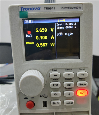
1: New circuit board, connected to bqstudio, using VIN = 12V.

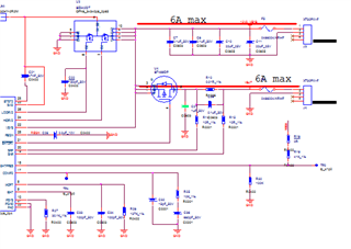
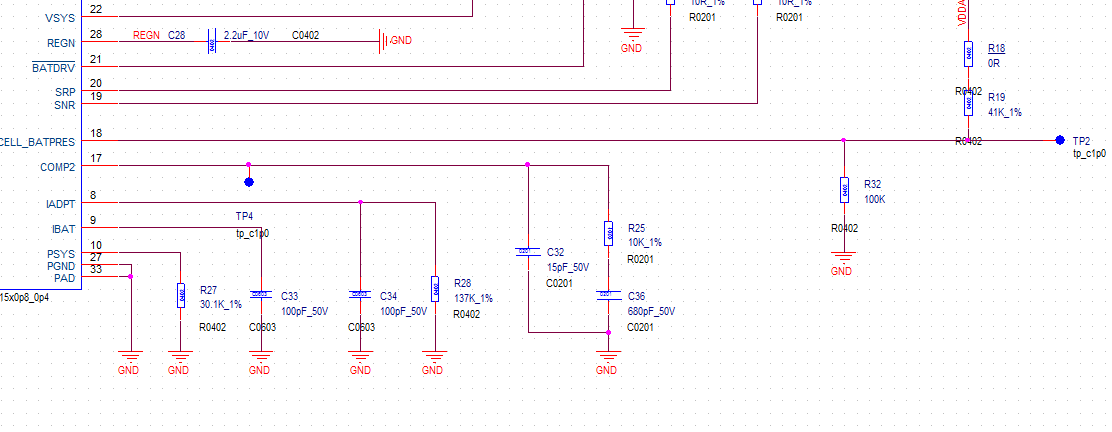
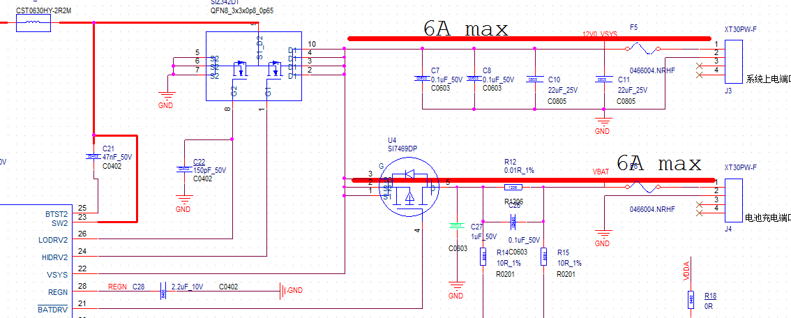
2: Use the divider to adjust the battery. The default is 4S battery. The circuit is as follows.

3: Connect a BMS board (without battery) to vsys and a load meter to Vbat.

4: The default parameters of bqstudio read chip are as follows:

Question 1:

1) At first, the parameters can be adjusted by communication, and the current can be pulled through the load meter.

2) When the pull current of load meter changes from 2.4a to 2.5A. The PMOS driven by batdrv has a high temperature instantaneously. By observing the register, it is found that it does not enter the fast charging mode, but enters the pre charging mode.

What may be the reason.

Question 2:

After the chip runs for a period of time (small current 0.5A, basically no heating), the communication is normal, but the read data is all 0000, which can be written through BQ, but it becomes 0000 again after re reading.

The measured regn voltage is 0.8V, not 6V. At this time, vsys = 11.6v, Vbat = 11.6v, these two voltages cannot be adjusted through BQ communication.

What may be the reason.

Question 3:

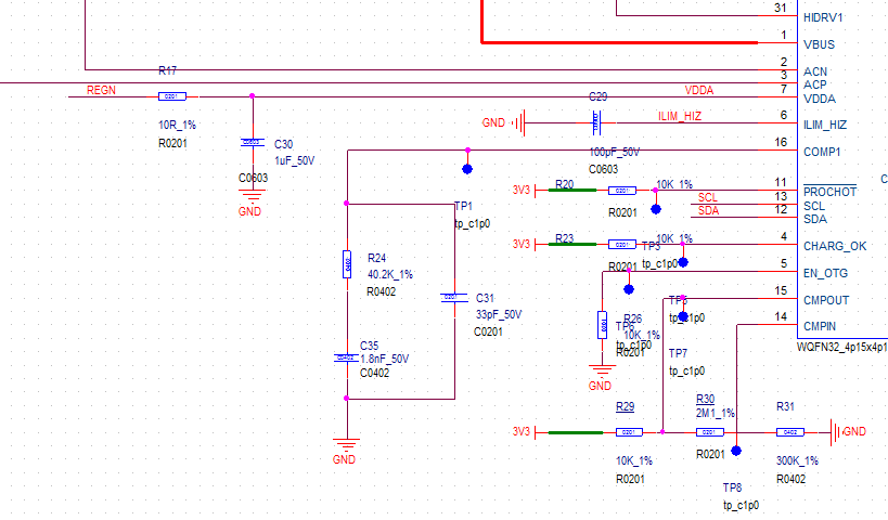
I use the independent 3v3 DCDC chip to supply power to 3v3 in bq25703a chip, and refer to the demo board circuit.

When bq25703 is not charged, the temperature of DCDC chip is normal. When bq25703 is charged, 3v3 will be high temperature with the increase of charging current.

Excuse me, under different external charging current, will the load of bq25703 taking power from 3v3 increase sharply?

  • Hi Jie,

    Thanks for reaching out. A couple of questions from me:

    1. "Connect a BMS board (without battery) to vsys and a load meter to Vbat". What do you mean a BMS board? For BQ25703A, system current is discharged on the VSYS node.

    2. Related to question 1, on what node are you pulling current from?

    3. What is the circuit operating condition in terms of input voltage, system voltage, system current, battery voltage, battery charge current?

    4. Is the charge current at 384 mA when you entered pre-charge mode? What is your operating conditions (refer to question 3 above)?


    To answer your questions and more questions:

    1. If your minimum system voltage is set too low, the system will enter pre-charge mode as the battery voltage is too low.

    2. What registers are you reading? REGN is only on when VBUS is present. If no VBUS is present, then your VSYS = VBAT.

    3. It should not change so much for an LDO to heat up. Most LDOs are capable of >100 mA range. Is anything else connected to the LDO?


    In your case, I think it will be a good idea to get an EVM and compare. 

    https://www.ti.com/tool/BQ25703AEVM-732 

    Thanks,

    Peng

    *If my answer solves your question, please press "This Resolved My Issue" on the thread.  

  • Hi Zhu:

    Thank you very much!

    1. "Connect a BMS board (without battery) to vsys and a load meter to Vbat". What do you mean a BMS board? For BQ25703A, system current is discharged on the VSYS node.

    I use DC source to supply the VIN, the voltage is 12V, and output current limit 10A.

    Use vsys to supply power to the next circuit board (BMS board),I used  CELL_BATPRES pins (75% of VDDA) to configure the number of voltage strings four series,and I want the voltage to be kept at 12V。

    Vbat is used to charge the four series batteries. The charging voltage range is 8V ~ 14.6v (LiFePO4 battery)

    2. Related to question 1, on what node are you pulling current from?

    Because I haven't prepared the battery at present, I hope to debug the circuit board first, so I use a load instrument to connect to the Vbat port, and then output the voltage and current configured by bqstudio through Vbat, and use the load instrument to pull the current (equivalent to charging the battery)

    3. What is the circuit operating condition in terms of input voltage, system voltage, system current, battery voltage, battery charge current?

    The following is the data after the chip is powered on:

    Charge Option 0 E20E
    Charge Current Register 00C0
    Charge Voltage Register 0550
    OTG Voltage Register 0000
    OTG Current Register 0000
    Input Voltage Register 0000
    Minimum System Voltage 2F00
    Input Current Register 4100
    Charge Status Register A000
    Prochot Status Register 0000
    Input Current Limit In Use 4100
    VBUS and PSYS Voltage Read Back 0000
    Charge and Discharge Current Read Back 0000
    Input Current and CMPIN Voltage Read Back 0000
    System and Battery Voltage Read Back 0000
    Manufacture ID and Device ID Read Back 7840
    Device ID Read Back 1078
    Charge Option 1 0210
    Charge Option 2 02B7
    Charge Option 3 0000
    Prochot Option 0 4A54
    Prochot Option 1 8120
    ADC Option 2000

    Then I set the Charge Current Register\ Charge Voltage Register\Minimum System Voltage\ and there VSYS VBAT NO change。From the software point of view, the communication is successful, and the data has been written。

    for example :

    1)When the chip is powered on, to measured vsys = 11V and Vbat = 11V 

    2)TO  change  Minimum System Voltage =14V,   Charge Voltage Register =10V ,Charge Current Register= 2A .but Vbat and VSYS no change.

    3) Use the load meter to pull out 100mA current, and the Vbat is pulled down to 5.6V

    4. Is the charge current at 384 mA when you entered pre-charge mode? What is your operating conditions (refer to question 3 above)?

     from the data , it does not enter the precharge mode。and VBUS=VIN=12V,the REGN should= 6V, but measured 0.8V。

    I want to know what changes in the internal operation of the chip when the external power supply is 2A or low current, or high current,?which leads to my normal charging with 2.4a. However, once it is adjusted to 2.5A, the PMOS has high heat?

    Thanks for your kind attention and look forward your prompt reply!

  • Hi Jie,

    I think I see what your problem is. First of all, I want to say that is not how you are supposed to test a battery system.

    If you connect a constant current load to the VBAT pin, then you have a E-load current loop fighting the charger's charging loop. In a battery charging system, the charging loop is dictated by the charger and charger only. Recommend to use a sourcemeter or a 4 quadrant power supply to test during the prototyping phase. Some people use a E-load in constant voltage to sink current (relies on the charger charging loop), but I haven't tried that myself.

    To test your BMS board that you are powering through VSYS, you should just use a regular benchtop DC power supply.

    To test the charger section, you should use a sourcemeter or a 4 quadrant power supply to emulate a battery during prototyping phase. Alternately, you can use a real battery, but that will involve some risks.

    "Then I set the Charge Current Register\ Charge Voltage Register\Minimum System Voltage\ and there VSYS VBAT NO change。From the software point of view, the communication is successful, and the data has been written."

    It seems like you have some misunderstanding of the charger operation. Charge current is a loop of the charger that determines the charging current. Charge voltage is the maximum voltage the charger will charge the battery to, it does NOT change the battery voltage instantaneously. VBAT voltage is determined by the battery only. Minimum system voltage is what the charger will try to regulate VSYS to but it does not change the VBAT voltage at any way. Please read about it on section 8.4.1.1 of the datasheet.

    I believe all your problems will be fixed if you have proper testing setup for a battery charging design. Recommend to use a new board since your old board may be damaged at this point.

    Thanks,

    Peng

    *If my answer solves your question, please press "This Resolved My Issue" on the thread.  

  • I'm glad to tell you that the problem has been solved.

    1) When using the load meter to test, use CV gear to pull the load current.

    2) In the circuit design, it is necessary to ensure the ripple of input and output. The ripple of input will be increased under load, which will affect the normal operation of DCDC chip.

  • Thank you again!

  • Hi Arvin,

    Glad to hear that your problem has been resolved.

    Best wishes,

    Thanks,

    Peng

    *If my answer solves your question, please press "This Resolved My Issue" on the thread.