This thread has been locked.

If you have a related question, please click the "Ask a related question" button in the top right corner. The newly created question will be automatically linked to this question.

TPS40077: Schematic review

Part Number: TPS40077
Other Parts Discussed in Thread: CSD17579Q3A, CSD17577Q5A, CSD17579Q5A, CSD17577Q3A

Dear team

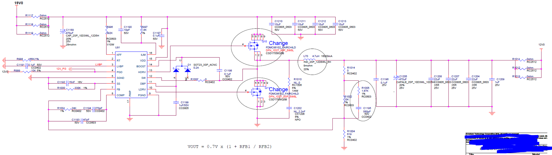
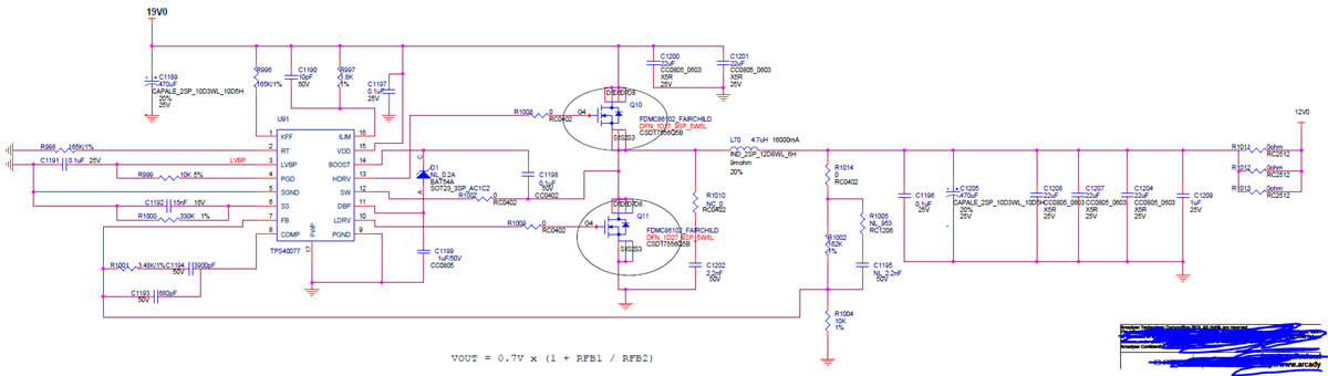
There is a good news that we design in TPS40077 in customer's new project.

The spec is Vin=19V,Vo=12V,Io=12.5A.

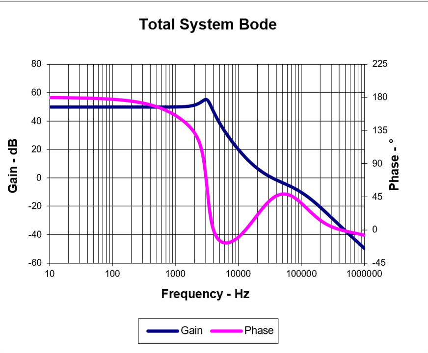
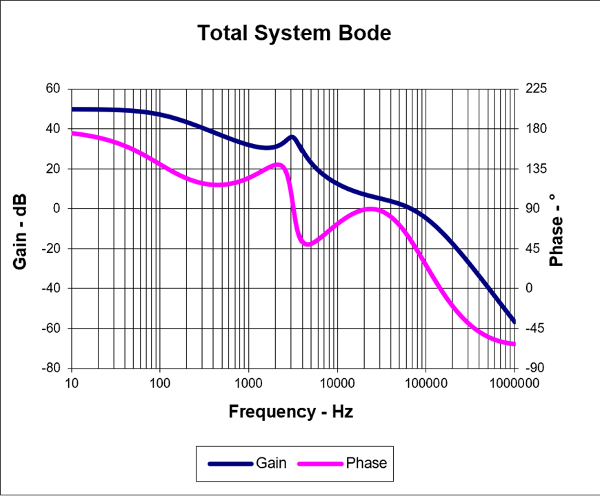
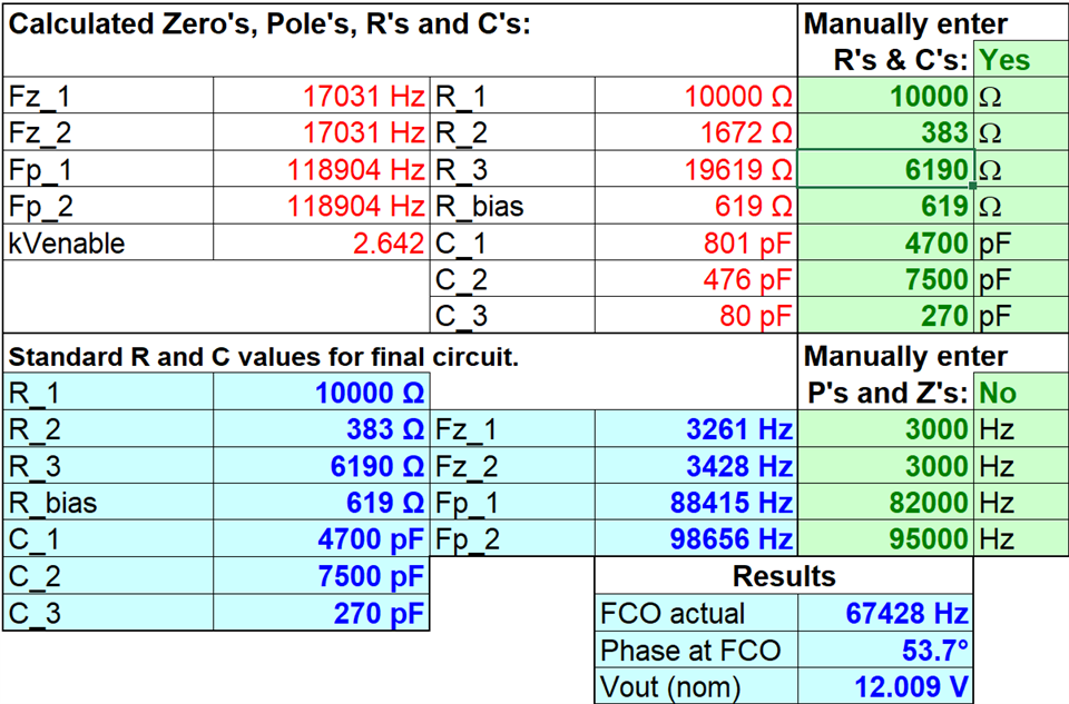
Could you help to review the schematic and recommend the solution of  Q10 and Q11.   

Many thanks

Denny

  •  

    To review the compensation, please use the compensation design tool - https://www.ti.com/product/TPS40077#design-development 

    Looking over the rest of the schematic:

    1) You have included series resistors on LDRV, HDRV and SW, but not one on BOOT.  If you believe you will need to be able to control the rise and fall timing of the switching node, you should include a resistor in series with the BOOT pin.  Place this between the IC pin and the D1 connection so that the recharge current from Driver Bypass (DBP) to the boot-strap capacitor (C1198) does not have to pass through the current limiting resistor.

    2) The UVLO level set by the KFF resistor (R996) is low for a 12V output.  WIth RT = 165k (300kHz) and RKFF = 165kHz, the UVLO level is 7.3V.  It is generally advisable to have the UVLO voltage set higher than the intended VOUT value.

    3) You asked about a recommendation for Q10 and Q11, but there are MOSFET part numbers listed.

  • Hi peter

    Thanks your recommend.

    3) You asked about a recommendation for Q10 and Q11, but there are MOSFET part numbers listed.

    - The customer just put a sample, could you help to recommend the solution of  Q10 and Q11 for this application?

    Many thanks

    Denny

  •  

    I have asked John Wallace, one of our experts from the MOSEFT applications team to help you with a MOSFET recommendation.

  • Hi Denny,

    I am the applications engineer for the FET product line. Peter asked me to make some FET recommendations. I'd go with 30V FETs in either 5x6mm SON or 3x3mm SON package and would consider CSD17579Q5A for the sync FET and CSD17577Q5A for the control FET. Both of these devices are available in 3x3mm package as well: CSD17579Q3A and CSD17577Q3A. On the MOSFET Support & training site, we have a FET selection tool for sync buck. I plugged in your requirements and these are the FETs I'd recommend. I have attached the spreadsheet for you to try out as well.

    Thanks,

    John Wallace

    TI FET Applications

    SYNC-BUCK-FET-LOSS-CALC_Rev1.xlsm

  • Hi John

    I appreciated your great support.

    Many thanks

    Hi peter

    The customer would like to confirm the parameter of excel file correspond to user's guide.

    The type III compensator refer from compensation design tool - https://www.ti.com/product/TPS40077#design-development 

    Type-III Compensation With the TPS40077 refer from datasheet page.29.

    1. Could you help to check the signal(Vo,FB and COMP) are right? 

    Many thanks

    Denny

  •  

    Yes, those are the correct connections.

    R1 in parallel with C1 + R2 are from Vout to FB

    Rbias is from FB to SGND

    C3 in parallel with R3 + C2 are from FB to COMP

    From the original schematic, as best I can read it.

    R1 is R1002 = 162k

    R2 is R1005 953

    R3 is R1001 3.48k

    Rbias is R1004 10k

    C1 is C1195 2200pF

    C2 is C1194 3900pF

    C3 is C1193 680pF

  • Hi Peter

    Thanks your recommend.

    The customer already modified the schematic.

    Could you help to review the schematic and compensator?

    The compensator as attached.

    TPS40KType III Loop Stability kVenable_sluc263c-071312_ARC_0706.xls

    1. You have included series resistors on LDRV, HDRV and SW, but not one on BOOT. If you believe you will need to be able to control the rise and fall timing of the switching node, you should include a resistor in series with the BOOT pin. Place this between the IC pin and the D1 connection so that the recharge current from Driver Bypass (DBP) to the boot-strap capacitor (C1198) does not have to pass through the current limiting resistor.

    =>Removed series resistors on LDRV, HDRV, only SW is on (according to the reference line)

    2. The UVLO level set by the KFF resistor (R996) is low for a 12V output. WIth RT = 165k (300kHz) and RKFF = 165kHz, the UVLO level is 7.3V. It is generally advisable to have the UVLO voltage set higher than the intended VOUT value.

    =>The customer used the following formula to calculate the Rkff value to be 392K and UVLO=17.1V

    Many thanks

    Denny

  • Hi Denny,

    Peter will feedback to you on Monday US time.

    Thanks,

    Lishuang

  •  

    The schematic looks better now.

    Looking at the compensation spreadsheet, I had to change the part number to TPS40077, and after doing do, I noticed that the phase margin at the L-C resonance is very low.  Looking into why, I can see a couple of issues:

    The ESR value for the 22uF ceramic capacitors is entered as 30mΩ, which is really high for ceramic capacitors, so I tried adjusting this to 3mΩ for a more realistic value.  Also, the L-C double pole is at about 3kHz and the loop's compensation zeros are set at 24kHz, so there is no phase boost at the L-C resonance.

    Using the manually enter Poles and Zeros feature, I set the poles down at the 3kHz L-C resonance to give phase boost at the L-C resonance, and I get a much better looking loop.  It also has higher bandwidth.

    TPS40KType III Loop Stability kVenable_sluc263c-071312_ARC_0706_PJM.xls