This thread has been locked.

If you have a related question, please click the "Ask a related question" button in the top right corner. The newly created question will be automatically linked to this question.

LMG1210: Getting the output at pin4

Part Number: LMG1210
Other Parts Discussed in Thread: SN74LVC2G17

Hi Team,

Can you please check and advise with following request?

"

I am working on LMG1210 EVM. 

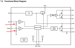
First, since the module is using an Schmit-trigger buffer I don’t expect to experience a difficulty in getting an output, but to our surprise getting the output at pin4 has been a challenge. Thus we think of bypassing it (buffer)  but it gave a similar challenge due to missing R31.

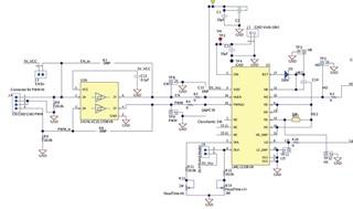
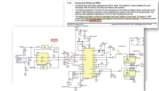
 From SNVU572- January 2018 document, section 7.3.3 bullet no. 3, there is a recommendation for bypassing the buffer IC (U2A). The R31 is clearly not present on the board. Placing the DNP resistors (R1 & R8) and removing the connecting resistors (R2 and R3) doesn’t make sense to me.  I have color coded the wording from the documentation wrt the actual location of components from schematic. An actual board photo has been put side by side with the EVM Assembly drawing and PCB layout snapshot showing the location of the R31 (yellow arrow)


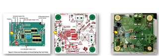
Hope to receive a response on this as generating an output from the module is not possible without getting the signal to the controller.

 "

Thanks in advance

Best Regards

Furkan Sefiloglu

  • Hi Furkan,

    Thanks for reaching out!

    ---------

    I agree that it does not make sense to remove R2 and R4.

    ---------

    To double check:

    1)  Is the LMG1210 in PWM or Independent Input Mode?  (Confirm by looking at J6)

    2)  Is the SN74LVC2G17 Schmitt-Trigger seeing sufficient voltage on its inputs?  For a 5V VDD,  at least a 2.5V high signal must be seen by the input pin.  So, please confirm that the function generator has a large enough signal coming from it and that it is powered up.

    ---------

    If the above does not fix the problem, you could consider de-soldering the SN74LVC2G17 and soldering wires directly on the R2 and R4 pads, or onto the EN and PWM "test points" that are vias on the board.

    ---------

    I hope this helps!  If this worked / answered your question, please press the green button.  If not, please feel free to follow up!

    Thanks,

    -Aaron Grgurich

  • Hi Aaron,

    Please find feedback as below:

    "

    Hi Aaron,

    Let me give my response on the points you have raised:

    Is the LMG1210 in PWM or Independent Input Mode?  (Confirm by looking at J6)

    { Yes, we would like to try the basic option thus we are using the PWM. J6 is open and J3 is shorted to PWM - I hope this is what you mean }

    Is the SN74LVC2G17 Schmitt-Trigger seeing sufficient voltage on its inputs?  For a 5V VDD,  at least a 2.5V high signal must be seen by the input pin.  So, please confirm that the function generator has a large enough signal coming from it and that it is powered up.

    { Yes, as you know in the PWM configuration Pin 1 of SN74LVC2G17 is tied to +5Vdc thru J3 jumper and this input voltage is coming from the LMG1210.  I can clearly see also a 5Vdc going to EN pin of LMG1210 thus the buffer is fine with steady DC input. PWM signal is also fine from my checking- I tried several clock shape as well but not getting the right output }

    We have ordered additional boards to check if this difficulty will be observed as well getting the output of PWM to the LMG1210. At the moment, for unknown reason the LDO of LMG1210 is no longer working thus it is not powering on the buffer. 

    Isolating the buffer from the circuitry (cut the trace from Pin5, and removed R2 and R4) ,  I have supplied the Vcc+5 from external PSU and tried PWM signal to both channels (one at a time) but did not get output from either of the channels. Steady DCin to either of the input pins will give an output.

    "

    Thanks in advance

    Best Regards

    Furkan Sefiloglu

  • Furkan,

    Thanks for the thorough response!

    It seems that you should be in PWM Mode.

    ----

    1)  For U2A (SN74LVC2G17), does Pin 3 see at least ~ 3V during the PWM_in on time??

    2)  When isolating the buffer from the rest of the circuit, are you providing sufficient PWM voltage?  (Have you confirmed with an oscilloscope?)  Consider putting the function generator output in the "High-Z" setting.

    3)  Maybe this unit was damaged from ESD, etc?  With the LDO not working, it is hard to decide what is wrong with the set-up.  Let's see how the new EVM units are.  Please let me know when those come in and how they react.

    Thanks,

    Aaron Grgurich

  • Hi Aaron, 

    Please see the feedback, 

    "

    For now, let us put this in pending. I will try to do some more standalone testing for the buffer. Peak to peak  clock signal is sure more than 3V at the input pin.

    I agree that this is now difficult to understand the reason why signal is not coming out of the buffer due to damaged LMG1210.


    For the RIPD question , where this table came from? If this is the suggested one for the buffer, the EVM has 20Kohms, if this is for the LMG1210 – there is none in the schematic


    Once we received the new boards, we will do a pin to pin signal checking.

    "

    Thanks in advance

    Best Regards

    Furkan Sefiloglu

  • Furkan,

    Understood; once you are ready, please respond to this thread or open a "related" thread to this one.

    -------

    And sounds good.  Hmmmm, interesting... Again, like you said, let's wait until we get the new units and see how they are.

    -------

    Regarding the R_IPD spec, that is found Section 6.5 - Electrical Characteristics.

    The resistors the R_IPD spec is referring are these ones:

    They are the internal resistors values within the IC.

    -------

    I hope this helps!

    Thanks,

    Aaron Grgurich