This thread has been locked.

If you have a related question, please click the "Ask a related question" button in the top right corner. The newly created question will be automatically linked to this question.

TPS61240: Could you review my schematic and board layout?

Part Number: TPS61240

Hello, 

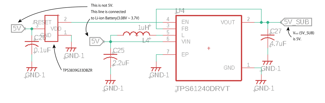
I have some questions about schematic and board layout with TPS61240.

The TPS61240 that I use for my project didn't work property.

I assumed the problem is a board layout, So I updated the layout.

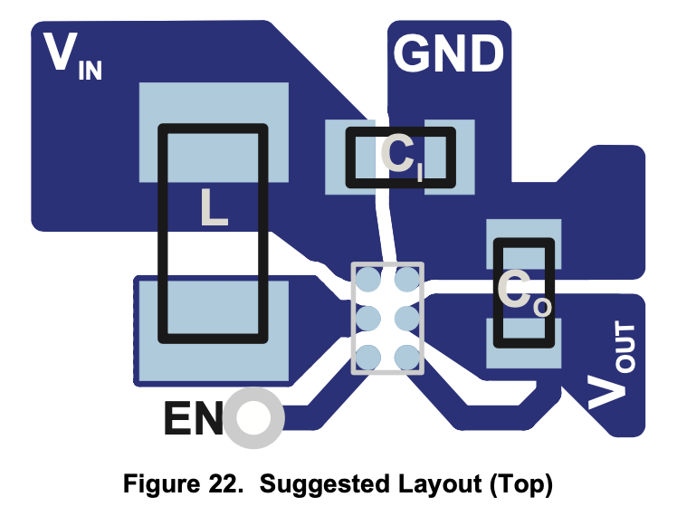
Could you review my schematic and board layout to prevent same mistake?

This is my schematic(fig1).

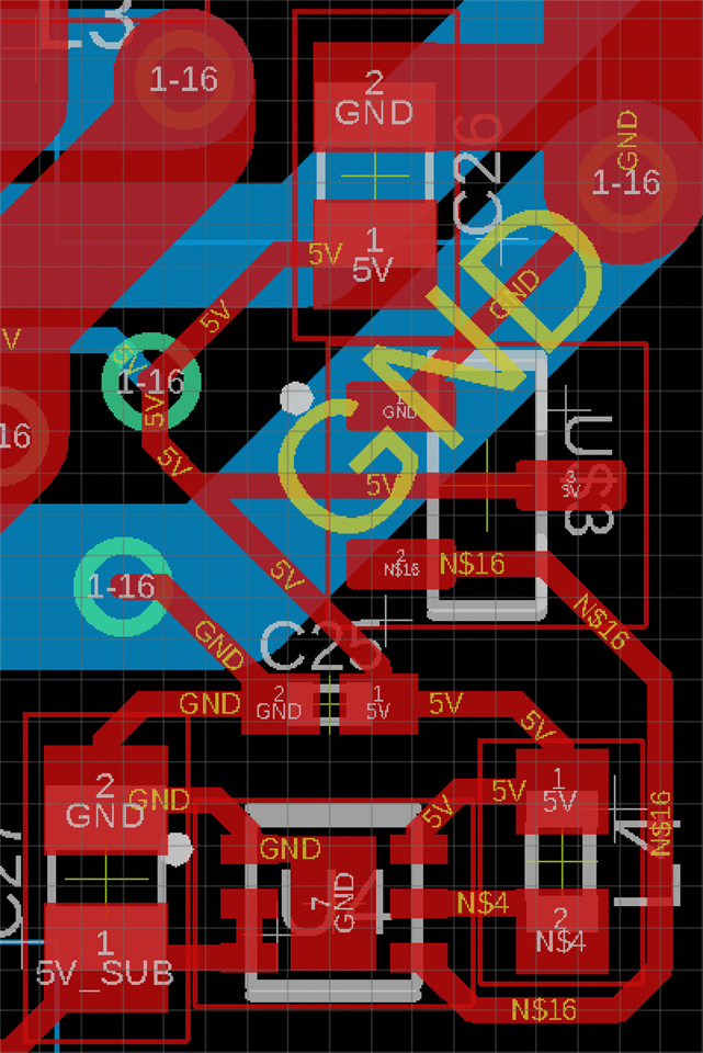
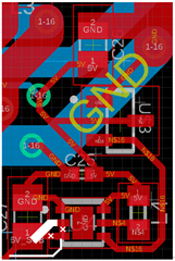
This is my board layout(fig2).

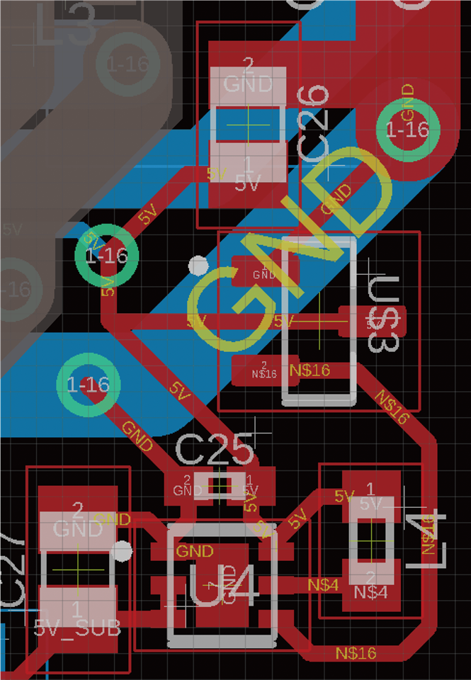
And if possible, Could you tell me where are no good in old board layout?

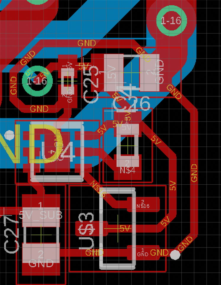
Old board couldn't step up voltage to 5V. It outputs 1.8V with huge ripple.

Click here to play this video

(Video URL : https://drive.google.com/file/d/1sYtx5l7J-lXN0-zgC8fz_RvAY9YLiDL9/view?usp=sharing)

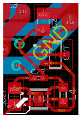
Old board layout(fig3).(Schematic is same.)

Thank you.

  • Hi N,

    Thank you for providing information. I actually think your old layout is better because it aligns more with out EVM recommendation and VOUT-GND loop is smaller in old layout. I strongly recommend you to refer to our EVM layout and do your modification.

    The schematic looks ok. Have you ever tested VIN when VOUT cannot start up? My best guess here is VIN is limiting its current when start up which makes VIN<UVLO.

    -Wenhao

  • Thank you for your reply.
    It's interesting that old board layout(fig3) is better than updated one(fig2). I modified the board layout(fig4). Which is better fig3 and fig4?

    By the way, I referred this layout(fig5). Is it EVM layout?


    I tested VIN in old board when VOUT cannot start up. VIN's voltage is 3.3V, current is 10mA. So, I think voltage is VIN>UVLO.
    I noticed that TPS61240 output 5V properly when I connect load to Vout after connected VIN a few second ago.
    Is there any other possible cause?

  • Hi N,

    Yes, you can refer to figure 22 in the datasheet which I think is good and similar to EVM. You can also check the application note: 

    https://www.ti.com/lit/an/slva773/slva773.pdf?ts=1624409094252&ref_url=https%253A%252F%252Fconfluence.itg.ti.com%252F

    This will note you how to design a good boost converter PCB. 

    For your new layout, see my comments below

    You cannot just connect VOUT to FB pin in that way. You should separate them. If you connected FB and VOUT before the COUT cap, all the noise from switching will couple to FB, which will make unpredictable behavior of the loop. Instead you should connect the FB after the COUT and connect VOUT to COUT directly.

    Remember the most important loop for a boost converter is SW-VOUT-GND loop. FB and anyother EMI sensitive component should not be in this loop.

    -Wenhao

  • Hi N,

    I add one cross on the layout, refer to below instead.

    -Wenhao

  • Thanks to your figure and comment, I realized the meaning of SW-VOUT-GND loop.
    I'm going to read the User's Guide.
    Then I'll make test board, and check behavior of TPS61240.
    If it doesn't output 5V properly, I'll ask again as "a related question".
    Thanks for your superb advise!