This thread has been locked.

If you have a related question, please click the "Ask a related question" button in the top right corner. The newly created question will be automatically linked to this question.

TPS650864: Technical issues

Part Number: TPS650864
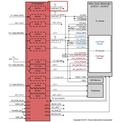
Other Parts Discussed in Thread: TPS650861, BOOSTXL-TPS650861

Hi team,

I got a question from customer.

The problem of tps6508641

1: Built in OTP can be programmed to control whether the output voltage of the power chip conflicts with the user operation register;

2: When the user operates the register through IIC bus, why does the corresponding power supply not output the corresponding voltage when writing the voltage value of buckxvid register; In addition to writing voltage value to buckxvid power register, is there any other operation;

3: The default device address of power chip is 0x5e. How to change the default device address of power chip;

4: Can I hang several power chips on an IIC bus?

5: Whether the output voltage of the buck1 of tps6508641 is 5V when it is powered on does not require any operation;


Thank you very much for your help.

Best regards,

  • Hello,

    Thank you for your questions - I will hopefully clarify some items.

    1. Built in OTP can be programmed in the TPS650861, not in the TPS650864 devices. The TPS650864 devices come with the one-time programmable memory already programmed. That said, the volatile user registers which are loaded from NVM can be modified after power up but will reset each time the OTP memory is reloaded (power cycle, fault, etc)

    2. There are a few potential reasons. BUCK1 for example is in ext fb, so the BUCK1VID registers don't do anything. BUCK3 uses CTL6 to choose between BUCK3VID and BUCK3SLPVID, so in that case you would need to change the correct register to see a response. However, the rest should be controllable with BUCKxVID registers, assuming that the PMIC is in stable operating state (not power faulting). If the PMIC is power faulting, then it will continuously reload OTP memory values, preventing I2C writes from sticking

    3. I2C_SLAVE_ADDR register is detailed in the TPS650861 datasheet.

    4. Yes, though it gets potentially tricky depending on how the programming is done. If the PMICs are programmed before solder down (using BOOSTXL-TPS650861 or buying pre-programmed from Arrow), then no issue. If the programming is done after soldering the units on the final board, then some care is needed. The programming register space is always located in I2C address 0x38, so to access only one PMIC at a time to change the I2C address, the CTL4 pin has to be pulled high on only one PMIC at a time. Example: PMIC1 has CTL4 --> 7V, then write the I2C_SLAVE_ADDR to 0x48 and program the PMIC. CTL4 for PMIC1 set back to GND, then CTL4 of PMIC2 set to 7V, it's I2C address changed, then it is programmed, etc - repeating as needed.

    5.The output of BUCK1 depends on the resistor divider used - it is intended for 5V but that requires the resistors to be set up to divide 5V down to 0.4V. 

    To help with the debug - I recommend following the steps in this FAQ: https://e2e.ti.com/support/power-management-group/power-management/f/power-management-forum/992402/faq-tps650864-regulator-is-shutting-down-or-measuring-x-lower-than-expected---what-is-the-cause?tisearch=e2e-sitesearch&keymatch=TPS650864#