This thread has been locked.

If you have a related question, please click the "Ask a related question" button in the top right corner. The newly created question will be automatically linked to this question.

TPS43340-Q1: BUCK1 controller with long traces

Part Number: TPS43340-Q1

I have mad an eval board for some tests on replacing an existing PMIC on one of our mainboards.

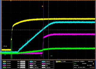
The BUCK1 controller won't start properly to regulate to 5V, just 0.3V are on the output.

After controlling the complete circuitry i found out the FET driving signals seem to be very sensitive.
So when playing around on GL1 with measure tips sometimes the channel gets working.

Since this channel has an offset FET with some distance of about near 100mm i wonder if there are other special recommendations on the routing?!

I guarded signal lines within an inner layer between grounds and avoided noise where possible.

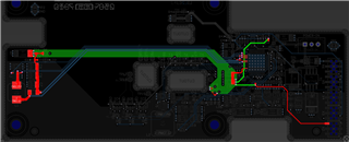
Are there measures to improve drive strength or something similar?

What workarounds could be tried before putting the PCB to re-design?

Thx for the help in advance!

  • Hi Markus,

      Can you try to cut the GL1 trace on the board and use a stronger wire to drive the FET before putting the PCB to re-design? 

      The FET should be placed as close as passible to the controller to make all driving signals as short as possible, since all gate driving outputs have high peak currents to drive capacitive load; themselves are switching signals with much switching noise.

    Thanks!

    Phil   

  • Hello Phil,

    i could not cut of the pcb traces due to the routing, but i added some additional 0,5mm wires on the bottom layer for GH1, GL1 und PH1.

    This seemed to do the trick  - though the outputs of BUCK 1 and 2 seem both to be very noisy.
    I expect that to be better when getting this in a optimized design. (Btw, there will be no re-design of eval pcb but immediately the design-in on our mainboard)

    This brings me to the question of design guidelines.
    We hadn't such problems with our former PMIC with offsetted FET's at the point of load - in my eyes one of the great advantages in PCB layout freeness when using BUCK controllers.
    I see the need of thick traces as short as possible and i think i can adapt our mainboard to get a similar placement like Evalboard.
    But would you provide a expectation of a maximum length/trace thickness?

    Topic #2 that was not finally tested an we discussed in a former thread was about the BUCK3 tracking BUCK1
    I'm not sure if it was clear that i have to source BUCK3 from BUCK1 due to the 4-10V input restriction - in my eyes a very unfortunate recommendation when having a 12V supply :-(
    So i think i cannot get BUCK3 tracking BUCK1 since BUCK3 will not work until VSUP is above 4V. At least i can obtain tracking from 4-5V!
    I got a plot of this:


    Best regards
    Markus

  • Hi Markus,

     The gate driving traces should be less than 10mm and 10mil minimum thickness in 1oz copper. 

      The major advantage of BUCK controller is giving much wider DC load capability.

      Since the 12V supply from car battery could have a glitch which level could be more than 24V, so, it can't be used to supply BUCK3.  

      Yes, BUCK3 can trick BUCK1 from 4-5V if it's ok for your design.

    Thanks!

    Phil