This thread has been locked.

If you have a related question, please click the "Ask a related question" button in the top right corner. The newly created question will be automatically linked to this question.

UA78L: Microcontroller and Level-Shifting Circuit Design

Part Number: UA78L

Hello. I am a young quality engineer and recently I have ran into a project where the best method for finding the root cause it to check everything off my long list of circuit design problems. The specific part that is currently in question and in the circuit is UA78L05ACDR.

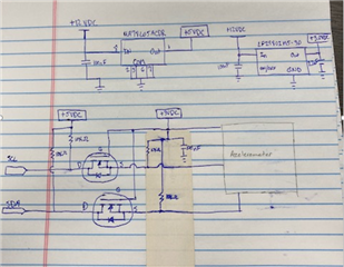
This design is older so they are use the regulator to drive MOSFET(s) (instead of chip) for the level-shifter (drain side of MOSFET). The same regulator is driving the microcontroller, which also drives an I2C signal to the drain side of the level-shifter. (These are the SCL and SDA signals in the picture.) I seen on the datasheet under section 8.2.2, figure 7 refers to the the layout on the datasheet when driving a level-shifter. Since the regulator drives both the microcontroller and this level-shifter (MOSFETs), I was curious if this layout in figure 7 is encouraged or discouraged based on what I have described? I was am also curious on what are the repercussions are for not setting the regulator up in this format? The datasheet states "This protects the regulator from output polarity reversals during startup and short-circuit operation." I was hoping someone could explain this to me in better detail or other problems that may arise because the circuit is not set up in the same manner as Figure 7 on the datasheet. 

I have attached a picture below of the main part of the schematic (hopefully it is clear enough) to help assist with what I described above. 

  • Please allow 2-3 business days for us to review all the details and get back to you. 

  • I recommend that you do place the diode to follow the datasheet in order to protect the UA78L05.

    Because the output of the IC is tied to the Level-shifter and data signals, the diode protects from reverse current situations as stated in the datasheet as you mentioned. Due to these signals both being not fixed, and not tied to a ground, Changes in these voltages, upon startup or transient operating conditions, could force a negative voltage or reverse polarity voltage(Vout>Vin) upon the LDO.

    In the negative voltage case, the added diode would allow for an additional path from ground to the negative rail on the output instead of sourcing from the LDO which would cause an overcurrent, short-circuit condition on the LDO and could cause shutdown or in extreme cases a possible failure. In the case of reverse polarity, the high potential across the BJT would result in current flowing into the emitter causing damage to the device, but with the additional diode, that voltage would be clamped, providing additional protection on the BJT element possibly saving the part assuming the output once again regulates to within operable ranges. However based on the schematic you have provided, I do not believe that reverse polarity voltage is a concern for this application.