This thread has been locked.
If you have a related question, please click the "Ask a related question" button in the top right corner. The newly created question will be automatically linked to this question.
Hello,
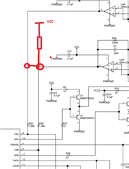
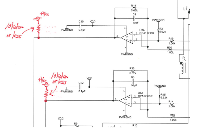
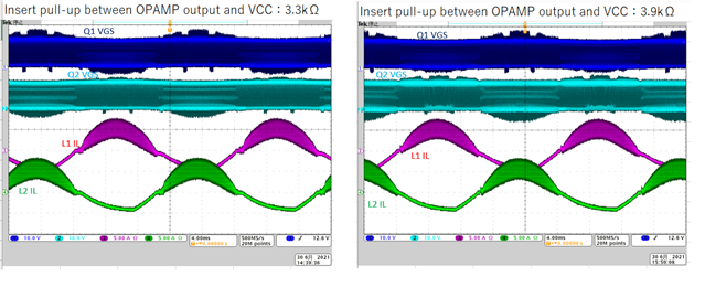
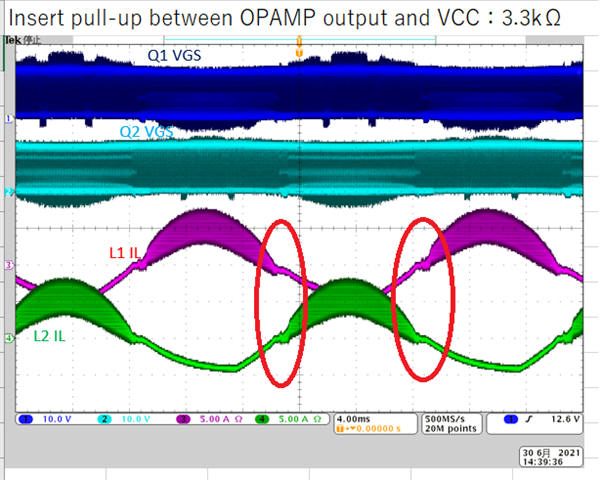
I have verified the operation of the bridgeless circuit of UCC28070, but confirmed the strange operation.
I have put together the questions in the attachment, so please let me know what you think.
Best regards,
Hi Kaji,
for your question 1, Do you mean the current spike on the PFC inductor?
if yes, it is usually caused by offset of the amplifier in the controller for current csa/csb. you should be able to add offset on the CSA/CSB to reduce the current spike.
please refer to SLUA479B application note(you can find it in TI website) for the offset design(ROA/ROB).
for your question2,
yes, once the Q2 flow from negative to the positive, the CT on the this leg can not sample the current correctly so the this current loop become saturation and output DMAX duty as the Dmax pin.
for real application, usually the DMAX is suggested to set below 95%. higher DAMX you set should help on the efficiency. But my understanding is it increase very little for example from 95% to 97%.
why we need a DMAX limited is that the Current transformer needs a time to discharge to avoid saturation.
Thank you for your reply.
I would like to ask you about offset adjustment.
This time, for current detection, a 0.05Ω resistor is inserted on the source side of the FET, the voltage across the resistor is amplified by OPA172, and then inserted into the CSA pin.
I referred to the reference design TIDA-0130A.
Is offset adjustment possible for the above configuration?
Best regards,
Hi Kaji,
sorry I can not find TIDA-0130A, can you please share it?
for your current detection with Resistor+ AP, I think it is a little hard to do the offset compensation because there are two amplifers in the sampling circuit (one is on the outside, the other is inside the controller). You can try to see whether any improvement.
keep in mind, you can improve it, but you can not remove it.
if the current spike influence the system spec like ithd, then try to add offset here.
The materials of TIDA-0130A are attached.
JOHN GRIFFIN has been created.
By the way, before, my question about UCC28070 was answered by JOHN GRIFFIN.
If I use this circuit, please let me know if there is a way to add an offset.
Best regards,
Hi Kaji,
you should also be able to add the offset voltage there. you can start with a resistor 10kohm, then step by step to decrease the resistor to see the improvement of zero crossing distortion.
Thank you for your reply.
Should I insert a pull-up resistor of about 10kΩ between each OPAMPS output and VCC?
See attached circuit diagram.
In the drawing you showed, it looks like you're shorting the outputs of both OPAMPS and pulling them up to VCC.
Best regards,
Hi Kaji,
sorry for my mistake.
you already get the point and your capture is correct.
I have verified the offset of CSA / CSB.
Certainly, the insertion of a pull-up resistor improved the superimposition characteristics near the zero cross.
The waveform is attached below.
With the 3.3kΩ pull-up, it does not overlap, but it looks slightly distorted as an AC waveform.
With the 3.9kΩ pull-up, the AC waveform is close to a sine wave, although there is some superposition.
I think it's better to use a resistance value around 3.3kΩ or 3.9kΩ, but let us know what you think.
Also, is it appropriate to connect a pull-up resistor to VCC?
Looking at the absolute maximum rating of the device, CSA / CSB is -0.5 to + 7V.
I know that VCC is about 12 to 15V, so I am concerned that it will exceed the maximum rating.
I think the pull-up resistor should be connected to VREF instead of VCC, but let us know what you think.
Best regards,
Hi Kaji,
It good to help the news that the offset can help on the current spike. You can select a resistor between 3.3k and 3.9k if use VCC as source of offset.
it is not problem when add offset from VCC since the voltage on the offset voltage is still under the maximum voltage 7V.
you can also use Vref and find tune the pull up resistor again.
Please tell me one more point about adding offsets.
The method you taught me is to pull up from VCC.
However, there are both pull-up and pull-down methods for adding offset in a normal circuit.
Is it necessary to add a pull-down resistor from VCC in this circuit?
Later, I'm thinking of pulling up with 3.3kΩ.
As shown in the figure below, are there any problems?
Is the operation of the red circle okay?
Best regards,
Hi Kaji,
whether or not you need an offset compensation depends on the requirement of the system, like PF and ITHD.
there is no need for a negative offset here.
The red cycle from your attached is pretty good to me.
hope this helps you.