This thread has been locked.

If you have a related question, please click the "Ask a related question" button in the top right corner. The newly created question will be automatically linked to this question.

TPS62000: L pin (Switch Node) Max Rating

Part Number: TPS62000
Other Parts Discussed in Thread: TPS62824A

Hi TI,

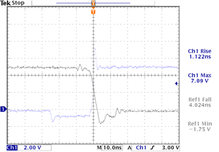
The L is rated at a max of Vin+0.3V. I have a 5V input and 1.2V output, but I am seeing a 6.8V spike at my L/SW pin, probably due to parasitic inductance. Is this already violating the spec? It's <2ns.
  • Hello Hao,

    It is expected that there will voltage spike on SW pin, however we don't have data to confirm if a 7.09V is acceptable because it's quite an old device. Anyway, typically a voltage with pulse duration of <10ns should be fine. Is the PCB layout optimize? Can you share it?

    By the way, are open in using a newer devices? Do you need a fixed frequency part or it is not critical?

    Best regards,

    Excel

  • This comes from an old design, so I am evaluating it. I have not check the layout yet. 

    I would prefer sticking to this device, as schedule is a top priority now. Of course if it's easy to replace i would welcome suggestions. I don't need a fixed frequency part, but preferably the part can operate in PWM mode constantly.

  • Hello Hao,

    If you intend to use TPS62000 on a new project, please ensure that the connection of the input capacitor to the VIN pin and SW pin to the output inductor is short as possible and with considerable trace thickness to minimize spike on the SW node.


    You can consider the TPS6280x (WCSP package) or the TPS62824A (QFN package) in your future projects. Both parts can operate in FPWM mode (quasi-fixed frequency).


    Do you have further queries?

    Best regards,

    Excel

  • Thanks for the suggestion. I have no further question.