Other Parts Discussed in Thread: LM7480, LM74800-Q1
Dear Team,
would You check if the schematic is suitable for the following requirements?
- VIn: 4,5-36V
- Max output current: 1,3A
- 1 minute at 42V
- ISO 7637-2:2011 Pulse 1:
-600V
Ri = 50 Ohm - ISO 7637-2:2011 Pulse 2a:
+50V
Ri = 2 Ohm - ISO 7637-2:2011 Pulse 2b
+20V
Ri = 0,05 Ohm - ISO 7637-2:2011 Pulse 3a
-200V
Ri = 50 Ohm - ISO 7637-2:2011 Pulse 3b
+200V
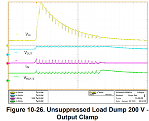
Ri = 50 Ohm - ISO 16750-2:2012 Pulsa 5a (Load dump)
+174V
Ri = 2 Ohm
The circuit should limit the output voltage to 40V during the 42V input test too.
Thank You in advanceLM7480.pdf