This thread has been locked.

If you have a related question, please click the "Ask a related question" button in the top right corner. The newly created question will be automatically linked to this question.

Question on TSP54310 AGND and PGND

Anonymous
Anonymous
Other Parts Discussed in Thread: TPS54310

Hi All,


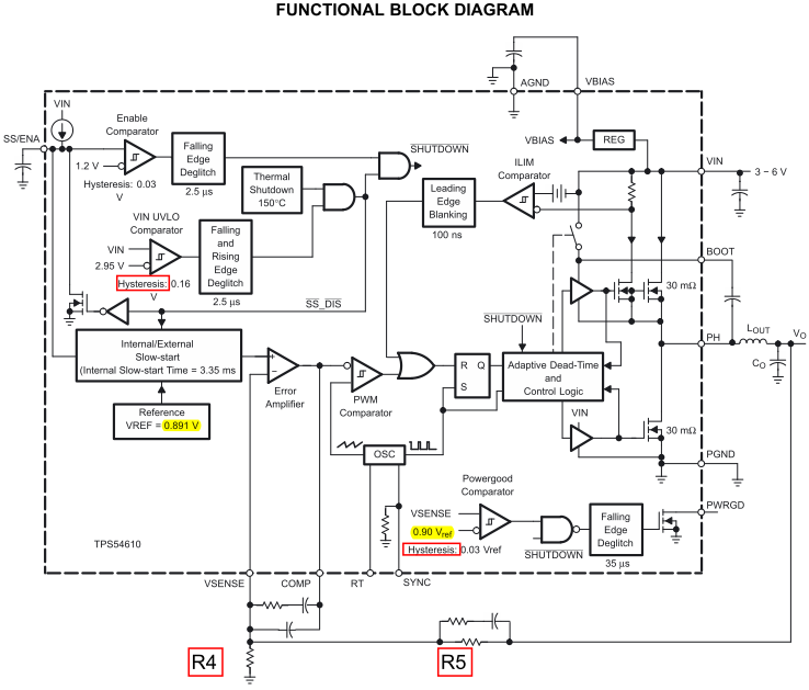
I would like to ask a question on TPS54310.


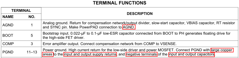
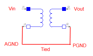
There seems to be two ground: analog ground and ground here. But in the PCB layout I see they are actually all tied together. Why?


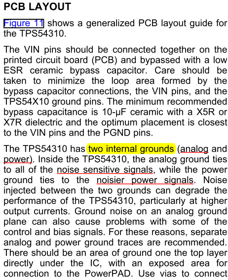
And on page 9, PCB Layout, internal analog and power grounds are said to have different functions and are connected to different (noise sensitive signal, noisier power signal). But since in PCB layout the two grounds are physically tied together, how can they differentiate then who is tied to noise sensitive signal and who is tied to noisier power signal?


Thanks,

Zheng

  • Yes, you will need to tie AGND to PGND at one point.  I recommend right at pin 1.  If the grounds are connected at a single point, no circulating currents can occur.

  • Anonymous
    0 Anonymous in reply to JohnTucker

    Dear John,

    Could you explain in detail the questions I have asked, especially how do AGND and PGND differentiate "noise sensitive signal" and "noisier power signal"?

    And what do you mean by "circulating" current? When will there be circulating current? Could you explain in more detail?

    And

    JohnTucker said:

    Yes, you will need to tie AGND to PGND at one point. I recommend right at pin 1.

    They are not tied at pin 1 in TPS54310 EVM PCB,  but instead are tied together to the large GND2 (this what the PCB file names the net) ground. So is this different from what you said?


    Zheng

  • I did not design or lay out the TPS54310 EVM, so I cannot directly comment on the techniques applied by the designer.  However it looks to me like there is only one ground net named GND2.  It is connected to AGND at pin 1.

    I take it from your questions that you are not familiar with switching power supply design.  In  switching dc/dc synchronous converter, ther are high current paths in the topology that trasmit power from the dc input to the dc output.  When the high side switch is on, the current flows from vin, thru the high side switch to the output inductor.  The AC current is shunted to ground by the output filter capacitor, while the dc portion is supplied to the load and also returned to ground. when the low side switch is on the conduction path is from ground thru the low side switch to the inductor.  So these are the power ground paths.  They are considered noisy as the switching currents in teh high and low side FET have very fast slew rates.  These fast di/dt's can interact with normal PCB parasitics to generate a fair bit of noise especially at higher current levels.  There is also analog control circuitrs such as the erroamplifierr, RT clock pin slow start circuit etc.  These are low level signals that are sensitive to noise.they are best termonated to an isolated "quiet ground" separate from teh power ground.  This is good design practice, but not always necessary, especially on lower current designs.  Since all the ground signals are "common", they need to ne at the same potential.  Tying them together at a single point does this.  to allow circulating current between analog and power ground, they must be conected together at more than one place to allow for a "return" path.


    I hope this makes your concerns clear.

  • The ratio of high side on time to switching period (1/Fsw) is the duty ratio D.  That is determined by the TPS54310 and is approx D= vout / vin.

    The regulated output voltage is there for any load circuits that may be attached, there is no differentiation between analog loads and digital loads.  No secret magic to time share.


    The power and analog grounds are local the TPS54310  PGND is for the switch returns, AGND is the return for the internal analog circuitry.

  • Anonymous
    0 Anonymous in reply to JohnTucker

    Dear John,


    May I use such analogy for AGND and PGND of TPS54310?


    JohnTucker said:
     
    The ratio of high side on time to switching period (1/Fsw) is the duty ratio D.  That is determined by the TPS54310 and is approx D= vin / vout.


    The ratio should always be smaller than 1, so Vin/Vout < 1, therefore Vout is always larger than Vin? But this is unreasonable since this would then make TPS54310 always an voltage-increase regulator, so how could it handle conversions like 5V to 1.8V?


    Zheng

  • It was late when I responded last night.  I fixed the D = Vout / Vin.

    Your analogy is similar, but what you show is more correctly "primary ground" and "secondary ground" for an isolated converter.  But yes there are two grounds that are meant to be tied together.

  • Anonymous
    0 Anonymous in reply to JohnTucker

    Dear John,

    Thanks for the clarification on Vin/Vout.


    JohnTucker said:

    When the high side switch is on, the current flows from vin, thru the high side switch to the output inductor.  The AC current is shunted to ground by the output filter capacitor, while the dc portion is supplied to the load and also returned to ground. when the low side switch is on the conduction path is from ground thru the low side switch to the inductor.  So these are the power ground paths.

    They are considered noisy as the switching currents in teh high and low side FET have very fast slew rates.

    1. In most cases I think people uses DC battery, or adaptor, none of which are AC source. So regarding "AC current", do you mean the AC element of the total current, which might vary so that there will be AC portion generated, but whose primarily/characteristic voltage/current is still DC?

    2. Regarding the "high side" "low side", could you sketch them in the following picture? When you say "FET", do you mean those 30mOhm FETs on the right of the image? There are four of them, so are the two on the upper "high side", and the two on the lower (one at PGND, one at PWRGD) low side?

    3. Why there are no FET close to AGND (on top of the diagram)?

    JohnTucker said:

    Since all the ground signals are "common", they need to ne at the same potential.  Tying them together at a single point does this.  to allow circulating current between analog and power ground, they must be conected together at more than one place to allow for a "return" path.

    I still don't understand what "circulating current" and "return" path are. Could your explain them in more detail, better with some pictorial illustration?


    Thanks,

    Zheng


  • Nice explanation. But in one instance, You are suggesting to isolate the  "Quiet"  Analog ground from Power Ground, but your are conflicting this by suggesting to tie both the grounds common .  Please elaborate it, When it should be isolated?

  • For switching power supplies there are circulating current paths on the input and output. The GND (PGND) portions of these circulating paths tend to be noisy. Some converters provide for a separate analog (AGND) ground. This is used to terminate sensitive analog circuits. The idea is to keep this separate from the noisy PGND but to keep it at the same GND potential it is connected at a single point. With a single point connection, no current can flow from the PGND to AGND as for current to flow a second connection or return path is required.