Hellow,
I am thinking about how to generate a Power Good signal for the adapter input on a system using the BQ24172.
If I look at the common source of the input power switch, I think I can make a Power Good decision.
Please let us know your opinion on whether the monitoring method (draft 3 in the figure below) is appropriate.
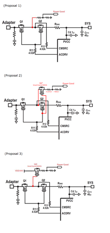
(Proposal 1) Method of directly dividing the common source by resistance
It worked fine in the experiment.
However, the description of the CMSRC pin in the data sheet has the following description.
"The resistance between ACDRV and CMSRC should be 500 kΩ or bigger."
Does the load resistance have any effect because it does not directly connect the ACDRV and CMSRC?
Please give us your opinion on this point.
(Proposal 2) Place a small signal NMOS (Q2') in parallel with the backflow prevention FET (Q2).
Considering the body diode, it is not much different from Plan 1.
By parallelizing Q2 and Q2', the topology is not changed.
There was no problem in the experiment.
(Proposal 3) Drive a small signal NMOS(Q3) with a common source
The power supply for Q3 uses the step-down DCDC output (about 4V) in the subsequent stage.
The gate of Q3 is overdrive, so it works as a simple switch.
There is no additional DC load when viewed from the common source.
It worked fine in the experiment.
However, when I connected the adapter with the battery, a spike-like fluctuation appeared in Power Good for a moment before conduction.
Best regards,