This thread has been locked.

If you have a related question, please click the "Ask a related question" button in the top right corner. The newly created question will be automatically linked to this question.

TL431: How TL431 can generate 2.5V reference voltage from a input voltage

Part Number: TL431

Dear TI team, 

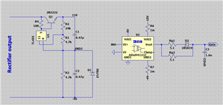
I have a bias circuit as below to generate +15V/-4V for a gate driver circuit.

During experiment and simulation, I noticed that under a certain heavy load condition, the TL431 lose control to generate +15V. Instead, it only generates +14.3V.

I check reference voltage of TL431, which is voltage across resistor R1, and see that the reference voltage is 2.344V, not 2.5V. 

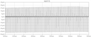
The current through TL431 seems very small as shown by the below waveform.

My question is:

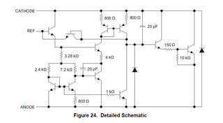
1) Just for a sake of my understanding, how TL431 generate its reference voltage of 2.5V from input voltage? Could you explain it by using the detail schematic of TL431 as below.

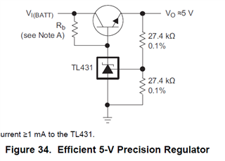
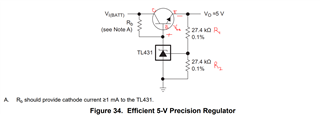
2) What is the reason TL431 loses its control? Is it because its current is very small (less than 1mA)? How should I solve this problem?

 Thank you so much. Regards

  • Hi Van,

    Thanks for your question. Can you please name the pins for on TL431 in the schematic for clarification? My thoughts below

    Best,

    Abhishek

  • Hi Abhishek,

    Thank you so much for your feedback. In the schematic, pin 6 is Anode, pin 7 is Cathode and pin 11 is REF pin for TL431.

    And why the current through Q1 is important for stability? I thought that current through TL431 is important (should be higher than 1mA).

    Also, could you please explain the principle for TL431 to generate a 2.5V reference based on its schematic in the original question? I think I need to understand it in order to understand the root of the problem.

    Thank you so much. Regards,

  • Hi Van,

    Thanks for letting use know the pin assignment of TL431 in the schematic. Can you please be specific about the load conditions in which TL431 does this? I see that your implementation of TL431 is the one shown in the datasheet's Fig 34. We can clearly see from the current graph that the current being provided to TL431's cathode is not sufficient, >1mA. There are few ways we can try fixing this issue. 

    1. Reduce R4 and see if we can provide more current to TL431 Cathode
    2. Replace TL431 with ATL431 to see if it gets the job done. We will need to adjust the R4 accordingly.

    Hope this helps in debugging the issue.

    Best,
    Abhishek

  • Hi Abhishek,

    Thanks a bunch for your reply. My load is a Gate driver circuit for SiC Mosfet with a given switching frequency.

    By the way, it is mandatory to have at least 1mA for Cathode current of TL431?

    Since in some simulations, I saw that with Cathode current less than 1mA, the output is still well regulated. Any disadvantage in this case?

    Thanks a lot. Regards,

  • Also, could you please let me know the method to calculate Cathode current of TL431 (formula relating input and output voltage, and resistance values)? For example, using Fig. 34 in the datasheet below. Thanks a lot! 

  • Hi Van,

    Great points. Below are the answers:

    • It is mandatory to have at least 1mA for Cathode current of TL431? -> Yes, that is the minimum cathode current we need to provide. You can see this in the footnote of Fig 34 also.

    • Since in some simulations, I saw that with Cathode current less than 1mA, the output is still well regulated. Any disadvantage in this case? -> If the current is lower than 1mA, then the reference voltage will drop and will not maintain.

    Best,

    Abhishek

  • Hi Abhishek,

    Thank you so much for your feedback. Can I know the formula to calculate the Cathode current?

    For example in the Fig. 34 about, can I say that Cathode current: Icathode = VI(BATT)/Rb? 

    Since when the output transistor of TL431 turns on, Rb is the only resistor connecting between VI(BATT) and GND.

    Thank you so much. Regards,

  • HI Van,

    It should be Icathode =  ((VI - (Vbe - Vo))/Rb - IB) where, IB is the npn base current, Vbe is the base-emitter voltage, and Vo is the output voltage = 5V in this case. Vbe is generally defined in the datasheet for npn transistors.

    I will also recommend looking into IE, the emitter current ie the sum of IB and IC (collector current). IE should be high enough to drive the feedback resistors. IE >= Vo/(R1 + R2)

    I hope this answers your questions. Please let me know if I can help with anything else. 

    Best,

    Abhishek