This thread has been locked.

If you have a related question, please click the "Ask a related question" button in the top right corner. The newly created question will be automatically linked to this question.

CSD95490Q5MC: Vsw with low load

Part Number: CSD95490Q5MC

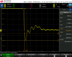
With low load our Vsw node seems to be out of spec. 

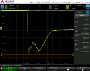
it seems to be out of spec upto 30A, but when i put 60A load, this ringing changes and it seems to be within spec. 

What to test, what to try? 

No snubbers on these pics, but does snubber affect that walley at low load. 

Will Boot pin added resistor have any effect on that?

  • Added: measured with 500MHz passive probe with short gnd spring

  • Hi Janne,

    The datasheet spec of -0.3V between VSW and GND is a DC spec which is to prevent high current flow through the body diode of LS FET if a negative voltage >-0.3V applied.

    The waveforms seem to be related to the VSW falling edge switching ringing within the deadtime period, the negative voltage supposes to be clamped by body diode of the LS FET, but there is parasitic inductance in the measurement loop which cannot be fully eliminated, The parasitic inductance caused the ringing. I am not concerned about the negative ringing waveform you attached.