This thread has been locked.

If you have a related question, please click the "Ask a related question" button in the top right corner. The newly created question will be automatically linked to this question.

BQ76930: BQ76930 charge query

Part Number: BQ76930
Other Parts Discussed in Thread: TIDA-01093

Hi

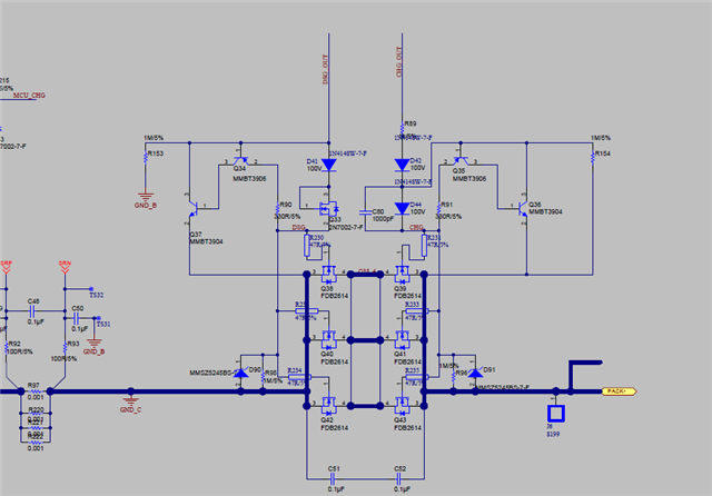
The customer design with two pieces of BQ76930 are cascaded to monitor 20S batteries.

The status of the CHG and DSG of the two BQ76930s read by the MCU, and then the MUC controls the logic chip (output 12V) to control the CHG and DSG MOS.

During the charging test, it was found that when the CHG MOS was turned off and the DSG MOS was turned on, the charger was able to charge; and the CHG MOS heated up, at this time Vgs=3.65V, Vds=3.6V; after disconnecting the charger, Vgs and Vds has no voltage. 

Please give some suggestion about this problem.

Thanks

Star

  • Hi Star,

    It looks like the design followed the basic structure of TIDA-01093 for a FET circuit.  The issue seems to be that they should have kept the Q31 of TIDA-01093 so that the charge gate voltage can fall with PACK- when a charger is applied.  As is, with the charger applied at a voltage greater than the battery and CHG_OUT low, the signal from the 12V logic chip which drives CHG_OUT can't go significantly below GND_B, perhaps -0.2V.  D42 and D44 will both be forward biased at perhaps 0.5V each putting the gate of the FET at about -0.6 to -1 V.  VGSTH of the FET is between 3 and 5 V, from the measurement about 3.65 V, so the FET will act as a source follower and the difference between the battery and charger will drop across the body diode of (Q42) and the charge FET (Q43) VGS.

    Include the P-ch such as Q3 in figure 8 of the BQ76930 data sheet or Q31 of TIDA-01093 after the 12V logic chip output.  This will allow the Q42 gate voltage to fall and Q42 etc to stay off when the 12V logic chip output is low.