This thread has been locked.

If you have a related question, please click the "Ask a related question" button in the top right corner. The newly created question will be automatically linked to this question.

TPS51200-Q1: I would like to get advice about TPS51200QDRCRQ1malfunction issue.

Part Number: TPS51200-Q1
Other Parts Discussed in Thread: TPS51200, , ALP

Hi everyone,

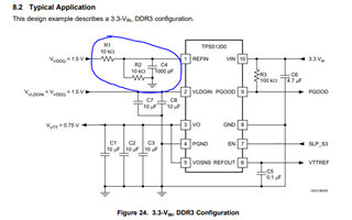
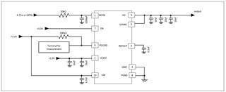
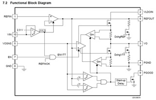
I use the TPS51200QDRCRQ1 device as the VTT regulator, that has 0.75V input at REFIN and 0.75V output from VO and REFOUT.

However, some boards were not worked correctly, even though same circuit has been build on every boards.  

The problem phenomena is same, the 0.75V was input at REFIN but 0.75V was not output from VO and REFOUT.

The OUTPUT of VO and REFOUT showed about 1V.

We do not think that that problem would be caused by the circuit.

Because the circuit is made as recommended circuit in the Datasheet, moreover there are some boards that worked correctly.

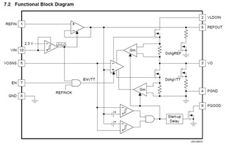
But we think that that problem might be caused by the input sequence of the REFIN/EN/VLDOIN/VIN pins.

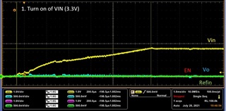
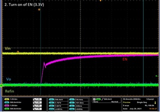
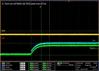
About the input voltage sequence of the REFIN/EN/VLDOIN/VIN pins, we are  understanding that there are no limitation.

But that problem might be occurred by resistance characteristic different of each boards, that means that problem would be caused by the input sequence difference of every boards.

So we would like to confirm that how should be set the TPS51200QDRCRQ1 device's the sequence of input voltages as the recommend condition. 

Would you please answer about the recommend input voltage sequence for TPS51200QDRCRQ1 device.

Thanks and Besr regards,

 Kura


  • Hi Kura,

    Can you provide waveform of REFOUT and VO to see if there is anything abnormal on the waveforms? If these waveforms are stable, they should follow REFIN. So we really need waveform to check if there is issue.

    Regards,

    Weidong

  • Hi Zhu

    Thank you for your reply.

    About your recommend of the waveform check, we can not provide and can not check the waveform right now.

    But our problem situation is that REFOUT voltage did not follow with REFIN voltage.

    When 0.75V volatge forced to REFIN, but REFOUT voltage is 1.05V, actually.

    We think about this problem wight be occurred by input voltage sequence.

    We think that our voltage input sequence would set as prohibit sequence and would  damage to the device.

    The input voltage sequence of TPS51200QDRCRQ1 on our board is almost same about following 5 pins.

       - REFIN input (0.75V)

      - EN input (3.3V)

      - VLDOIN (2V)

     - VIN (3.3V)

     - PGOOD pull-up (3.3V)

    However, those 5 pins are set as same time sequence, but slightly delay time might occur due to each wire resistance different.

    So I would like to know if the inhibit sequence of TPS51200QDRCRQ1 is on the REFIN/EN/VLDOIN/IN/PGOOD (pull-up) pins.

    Please give us the advice about the inhibit sequence of TPS51200QDRCRQ1 for REFIN/EN/VLDOIN/IN/PGOOD (pull-up) pins.

    Thanks and Best regards,

     Kura


  • Hi Kura,

    Regarding power up sequence, VIN has to come up earlier than REFIN, please refer to figure 19 and figure 20 for recommended power sequence. If REFIN is up before VIN, the internal state is not determined because lack of bias voltage, so it's possible to cause issue.

    Regards,

    Weidong

  • Hi Weidong

    Thank you very much for your quick reply.
    Your comment is really helpful for us to figure out our trouble.


    We would like to know about VO/VOSNS/REFOUT pin's output voltage level at following situations.
    Is there any possibility that VO/VOSNS/REFOUT pin's voltage would be measured higher than REFIN voltage at the following situations.

       - The situation 1 is: it apply about -0.7V level to VO pin from external power supply when VO is in the output state 0V.
         > VO pin level = ?     VOSNS pin level = ?     REFOUT pin level = ?

       - The situation 2 is: it apply about -0.7V level to VO pin from external power supply when VO is in the output state >0V.
         > VO pin level = ?     VOSNS pin level = ?     REFOUT pin level = ?

    Our problem is that REFOUT can not be measured as same voltage as REFIN.
    When 0.75V volatge forced to REFIN, but REFOUT voltage is 1.05V, actually.
    We would like to know why REFOUT is not same as REFIN, and what is cause of that problem.
    If 2 types situation above might be able to consider as the one of cause of our problem, we will check the repeatability of problem.
    Would you please give us your consideration about VO/VOSNS/REFOUT pins voltage about the 2 situation above.

    Thank you for your support as usual.

    Thanks and Beat regards,
    Kura

  • Hi Weidong

    Thank you very much about your support.

    Anyway, we replied to you about our question at few minutes before.
    However, we have some questions additionally.
    Please follow again about following questions.


    We would like you to give your comment about next question additionally.
    Would you please answer about our questions not only following questions, but also last our replay.

    [Additional question 1]

        Now, we faced on the new situation that means REFIN < REFOUT = VO volatage value.
        We would like to know that whether the REFIN < REFOUT = VO volatage situation would be occurred in normal function, or not.
        If not, we want to know what is conceivable cause about REFIN < REFOUT = VO volatage situation.
        What do you think about conceivable cause about that ?


    [Additional question 2]

        About operation point of view, is there any function problem during long time operation when the REFIN pin would be kept OPEN condition ?
        The REFIN=OPEN situation would be recommended as normal operation, isn't it ?

    Thank you for your support as usual.

    Beat regards,
    Kura

  • Hi Kura,

    For additional question #1, it's possible that REFOUT and VO is higher than REFIN, but most of the time it's because TPS51200 is sinking current (meaning current is flowing from load to TPS51200). You can referring to figure 10 and figure 15 in datasheet.

    For additional question #2, if REFIN is open, then there will be no reference voltage to generate REFOUT and VO, so the part will not have output voltage and will not be functioning. So it's definitely not a recommended operation condition.

    Regards,

    Weidong

  • Hi Kura,

    If you pull VO to -0.7V with external power supply, and TPS51200 wants to pull it to 0.75V, then two power supply will fight for each other and the stronger one will win. I don't know what's the current capability of the external power supply, but TPS51200 does have current limit ~4A. So if the external power supply is stronger then VO will be pulled down, and VOSNS pin will follow. But in a normal case REFOUT should still follow REFIN. If VO is 0V, it the situation will be similar, VO might be pulled to a negative voltage by the external power supply. 

    Regards,

    Weidong

  • Hi Weidong

    Thank you very much for your 2 times reply.

    From now, we would like to reconsider our problem together with your comment, and would be made sure about the root cause.

    When we will need your help again, we will send the message about that in this thread.
    We will be grateful if you could support us at that time.

    Thanks and Beat regards,
    Kura

  • Hi Weidong

    We would like to talk about Additional Question-1 for more detail due to investigate the root cause of the REFIN < REFOUT = VO voltage situation.
    We are checking the TPS51200QDRCRQ1 functionality by the board that is built with peripheral devices.

    Firstiy,
       We checked the VO/VOSNS/REFOUT voltage as initial function with following input voltage condition.
       We confirmed that TPS51200QDRCRQ1 is worked correctly.

         Conditon :
            REFIN     = 0.75V
            EN           = 3.3V
            VLDOIN   = 1.9V
            VIN          = 3.3V
            PGOOD   = pulled up by 3.3V though 100kohm resistance

         Output's measurment result : we think that those are shown as ideal value.
            VO          = 0.75V (no load conditon)
            VOSNS   = 0.75V (no load conditon)
            REFOUT = 0.75V (no load conditon)


    Secondly,
      We changed the input voltage of the TPS51200QDRCRQ1 as below to check other circuit.
      REFIN was set as open, and EN was set sometime as GND, sometime as 3.3V.

         Conditon :
            REFIN     = OPEN
            EN           = GND or 3.3V
            VLDOIN   = 1.9V
            VIN          = 3.3V
            PGOOD   = pulled up by 3.3V though 100kohm resistance

         Output's measurment result : we did not checked that at that time.
            VO         = no data (no load conditon)
            VOSNS  = no data (no load conditon)
           REFOUT = no data (no load conditon)


    Thirdly,
      We checked again the VO/VOSNS/REFOUT voltage with following input voltage condition.

         Conditon : same voltage condition as initial check
            REFIN     = 0.75V
            EN           = 3.3V
            VLDOIN   = 1.9V
            VIN          = 3.3V
            PGOOD   = pulled up by 3.3V though 100kohm resistance

         Output's measurment result : the measured value is not same as initial check. 
            VO          = about 1V (no load conditon)
            VOSNS   = about 1V (no load conditon)
            REFOUT = about 1V (no load conditon)


    We think that the device does not work correctly at third check, because VO/VOSNS/REFOUT voltage are not same as REFIN.

    So we would like you to give your comment about following questions.


    (A) We are investigating the root cause of VO=VOSNS=REFOUT=1V at REFIN=0.75V.
         What do you think about that VO=VOSNS=REFOUT=1V at REFIN=0.75V situation is caused by the condition of secondly ?

    (B) We would like to know why VO=VOSNS=REFOUT<REFIN situation would be occurred.
         Do you know the mechanizm of the VO=VOSNS=REFOUT<REFIN situation.
         The VO=VOSNS=REFOUT<REFIN situation would be reason that PS51200QDRCRQ1 device internal circuit had been damaged, isn't it ?


    Sorry for many time support request, but we are really want to figured out this issue.
    Thank you for your support as usual.

    Thanks and Beat regards,
    Kura

  • Hi Kura,

    For step 2, how did you make the REFIN pin open? Do you have resistor divider and capacitor to GND on the REFIN pin as shown in the below picture? If you can provide schematic it will be more helpful.

    Regards,

    Weidong

  • Hi Weidong

    Thank you for your prompt reply.

    Now, we are checking about your question how we did make the REFIN pin open.
    And the circuit might not be able to show you, but we are considering to tell you about our circuit information by different method.

    After that, we will reply to you about those things above, please wait a while.

    Thanks and Beat regards,
    Kura

  • Hi Kura,

    Thanks for the update, we will wait for your further information.

    Regards,

    Weidong

  • Hi Weidong

    Sorry for late reply.

    I would like to answer about your two questions below.

      (Q1) For step 2, how did you make the REFIN pin open?
      (A1) The external power supply was connected to REFIN at TPS51200 device function check due to forcing voltage.
             But when REFIN pin would be OPEN, the connection with external power supply would be cut off.

      (Q2) Providing the schematic,
      (A2) We explain the pin situation of TPS51200 device in our circuit as next.
              We would like you to understand our circuit from this explanation, and we hope this explanation would be helpful to know the schematics difference of yours.

           *REFIN : It has 10k ohm resistor and has pull-down with 10000pf.
                          R2 in your circuit is not set in our circuit.
                          There is the reason why the R2 did not set in our circuit due to the special designation.

           *EN : The power supply is connect directly.
                     It is same pin situation as your circuit.

           *PGOOD : It is connected to VIN pin, and it has 100k ohm resistor after connection point.
                            There is expernal terminal to measure the PGOOD voltage.
                            It seems that it is same pin situation as your circuit.

           *VIN : It is connected to PGGOD pin, and it has pull-down with 4.7uF after connection point.
                     It is same pin situation as your circuit.

           *VLDOIN: It has pull-down with two 10uF.
                            It is same pin situation as your circuit.

           *VOSENS: It is connect to VO directly.
                             It is same pin situation as your circuit.

           *REFOUT: It has pull-down with 0.1uF.
                            There is no connection REFOUT pin, there is only pll-down.
                            It seems that it is same pin situation as your circuit.

           *PGND : It is connect to GND directly.
                          It is same pin situation as your circuit.

           *VO : It has pull-down with three 0.1uF that it is outside from connect point with VOSNS.
                     It is same pin situation as your circuit.

    If you could not imagine about our circuit from this explanation, please let me know.

    We would like to know the mechanizm of the VO=VOSNS=REFOUT<REFIN situation.
    The VO=VOSNS=REFOUT<REFIN situation would be reason that PS51200QDRCRQ1 device internal circuit had been damaged, isn't it ?


    Thank you for your support as usual.

    Beat regards,
    Kura

  • Hi Weidong

    This is very fast turn, because we have one more question.
    Sorry for bother you, but would you please help to figure out our problem.


    We have another phenomenon, the resistance of troubled device between VLDOIN to VO shows lower than normal device's one.

      (Q1) We would like to know why the resistance characteristics would be changed ?
      (Q2) Is there any possibility that it would be caused by measurement environment ?
      (Q3) Should resistance characteristics between VLDOIN to VO be stable ?
      (Q4) Whether the observation of difference by some TPS51200 devices should be problem, or not ?
      (Q5) What are the possible cause of the resistance characteristics difference between failure and good devices ?


    Sorry for my many questions, but we need your help to figure out our problem.
    Thsk you very much for your support as usual.

    Best regards,
    Kura

  • Hi Kura,

    I would still request you to provide the waveform of REFIN/REFOUT/VO for us to better understand your problem. Without waveform, it's difficult for us to know what could have happened. Do you have any concern with providing waveforms? 

    Also I assume you actually mean VO=VOSNS=REFOUT>REFIN in above statements?

    Regards,

    Weidong

  • Hi Weidong

    Thank you for your support.

    We are considering to provide to you the waveform, please wait a while to answer about that.

    And let me answer about your question below.
    -Also I assume you actually mean VO=VOSNS=REFOUT>REFIN in above statements?

    We would like to explan about the phenomenon, the resistance of troubled device between VLDOIN to VO shows lower than normal device's one.

    This phenomenon is not observed at VO=VOSNS=REFOUT>REFIN situation.
    This phenomenon is observed when resistance would be measured between VLDOIN and VO with other pins are OPEN.
    Moreover, we think as strange there is the value of measured resistance between failed and good device shows difference.

    So we do not know whether there is any relationship between VO=VOSNS=REFOUT>REFIN and resistance phenomenon.
    If you might make sense the mechanism about resistance phenomenon, please let us know.

    And we would like to have your comments for this resistance phenomenon about next questions.
    Would you please give your comment.

      (Q1) We would like to know why the resistance characteristics would be changed ?
      (Q2) Is there any possibility that it would be caused by measurement environment ?
      (Q3) Should resistance characteristics between VLDOIN to VO be stable ?
      (Q4) Whether the observation of difference by some TPS51200 devices should be problem, or not ?
      (Q5) What are the possible cause of the resistance characteristics difference between failure and good devices ?


    Thsk you very much for your support as usual.

    Best regards,
    Kura

  • Hi Kura,

    Can you provide the impedance measurement between the "good" and "bad" devices? The connection between VLDOIN and VO is an MOSFET, it's possible that there is some damage to the "bad" device. 

    It's difficult for us to analyze the root cause just by description. Can you either provide the waveform, or send the "bad" device to TI customer service for analysis? 

    Regards,

    Weidong

  • Hi Weidong

    Thank you for your prompt support.
    Your replay is sent on Sunday night, I really appreciate for your strong support.

    Anyway, we can not measure about the impedance value due to no measurement system.
    However, we would like to send our sample to analyze to figure out the cause.
    Could you please tell us what we should do to send our sample to TI customer service.

       - What we should do to send our sample to TI customer service.
         If we have to make the form to request that, please let me know the URL.

    And we would like to know about next items.

       (A) How much is the cost when we will request to analysis to TI customer service ?
       (B) In general, How long days does it take until finish ?
       (C) To request, we think only one sample will not be enough, so how many samples will be needed as generally ?
             At that time, will good sample be needed also ?
       (D) Are there any limitations to request to TI customer service ?
                i.e. We got TPS51200 devices from Japanese company, but it will need to get that device through TI sales Department directly...

       (E)After the request the analysis to TI customer service, can you know about that result, and can we able to discuss again with you about the analysis result ?

    Thank you very much for your support as usual.

    Best regards,
    Kura

  • Hi Kura,

    Please use the below portal to submit the request. Multiple devices will be better. I think after you submit the request, you should get an expected turn time about the analysis, 

    http://www.ti.com/support-quality/resources/customer-returns.html.

    Also just want to clarify that REFIN open is not a valid operation condition, so please avoid this in your future application.

    Regards,

    Weidong

  • Hi Weidong

    Thank you for your quick reply and prompt support.

    We have to discuss with procurement Division person to send the sample to TI customer service.
    Because, we need to confirm our supply chain about purchase of our TPS51200 devices.

    According to your URL's information, if we got the TPS51200 from non authorized TI distributor, we will not be able to send the sample to TI customer service.

    If so, we would like to ask again about failure mechanism by this thread.
    Could you please support again about failure mechanism by this thread ?


    Thank you very much for your support as usual.

    Best regards,
    Kura

  • Hi Weidong

    Thank you for your prompt support.

    We would like to confirm about last your comment immediately,
    This confirmation is vary important for us, could you please reply again.

    We get your comment as below.
         > Also just want to clarify that REFIN open is not a valid operation condition,
         > so please avoid this in your future application.

    We would like to ask again about REFIN conditon.

    The TPS51200 device is used in our circuit and it impremented on the board.
    We are doing many functionality checks for our board(product).
    And one of functionality check condition is set as the VIN/LDOVIN/PGOOD/EN/REFIN condition like follows.


         (connection order 1) EN = set to GND
         (connection order 2) VIN = force 3.3V voltage directly from 3.3V regulator
         (connection order 2) PGOOD = force 3.3V voltage from 3.3V regulator with 100K-ohm pull-up   
         (connection order 3) LDOVIN = froce 1.9V voltage directly from 1.9V regulator
          (no connection)        REFIN = keep OPEN conditon during this functionality test

    Accoding to your comment as top, you mentioned REFIN=OPEN is not valid, that mean REFIN=OPEN would be prohibited ?
    If REFIN=OPEN should be prohibited, the REFIN condition in functionality check condition above should be changed, isn't it ?

    We would like you to answer about next questions.

       (Q1) What do you think about whether our REFIN < REFOUT = VO voltage situation problem might be caused by REFIN=OPEN check condition ?

       (Q2) What do you think about the connection order in our check condition above ?
               Would our connection order above be prohibited ?
       (Q3) If our connection order above would be prohibited, is there your recommendation about connection order ?
       (Q4) If REFIN=OPEN should be prohibited, what condition would be recommended about REFIN pin ?
                i.e. Pull-down to GND, or Pull-up to some voltage ....


    Thank you very much for your support as usual.

    Best regards,
    Kura

  • Hi Kura,

    Again, please provide waveform for analysis. We don't know how you disconnect the power supply to REFIN, and don't know if there is any spike when the connection is removed. So it's hard for us to tell just by text description. 

    Regards,

    Weidong

  • Hi Weidong

    Thank you for your prompt support.

    We are confirming to provide the waveform data to you.
    And, according to the procurement Division person, our TPS51200 device was not get from authorized TI distributor, so we can not send our problem samples to TI customer service.

    Naw, Japan has a national holiday until weekend.
    We would like you to wait our replay about waveform providing, we will reply to you next week.

    Very sorry inconvenience situation.

    Thanks and Best regards,
    Kura

  • Hi Weidong

    Sorry long time no reply to you.

    We get the waveform picture about VO=VOSNS=REFOUT>REFIN situation.
    We can show 3 pictures.

    1st: After measurement setup, the picture shows at turn on of VIN.
            By measurement setup, EN,REFIN are connected to GND at external power supply internally.
            (= External power supply is not be forceing any voltage yet.)

    2nd: The picture shows at turn on of EN after VIN turned on.
            EN,REFIN would be connected to GND at external power supply internally.
            By measurement setup, REFIN is connected to GND at external power supply internally.
            (= External power supply is not be forceing any voltage yet.)
            And VIN voltage has been kept 3.3V by external power supply.

    3rd: The picture shows at turn on of REFIN after EN turned on.
            And the picture also shows that VO level(= about 1V) is higher than REFIN(=0.75V).
            VIN,EN voltage have been kept 3.3V by external power supply.
             VO is out at the timing of REFIN voltage forcing, but voltage level is different from REFIN.
            It should be same.

    Is there any abnormality about those pictures ?
    If you have any comment about that, please let us know.

    And we would like to explain about REFIN open situation additionally.

    Above three picures is taken at the maesurement setup condition that is following.
    Each pin has been turn on at respectively by manual operation of external power supplies.

      [Condition A]
         REFIN    = 0.75V by external power supply A 
         EN          = 3.3V by external power supply B
         VIN         = 3.3V by external power supply C
         VLDOIN  = 1.9V by external power supply D (No waveform picture)

    About REFIN open situation is almost samme, but setup condition is different as below.

      [Condition B]
         REFIN    = OPEN (Any instruments is not be connected.) 
         EN          = GND or 3.3V by external power supply B
         VIN         = 3.3V by external power supply C
         VLDOIN  = 1.9V by external power supply D

    The VO>REFIN phenomenon has been observed by REFIN=0.75V condition(=condition A) after functionality check for other device (not TPS51200) on the board.
    That functionality check is done about several condition. And some of that include REFIN=OPEN condition(=condition B).


    We would like to know about the relationship between VO>REFIN phenomenon and REFIN=OPEN situation.
    If you have any comment about that, please let us know.


    Thanks and Best regards,
    Kura

  • Hi

    REFIN=OPEN is not a valid operation and the device is undetermined under this case.  

    We recommend at least 20uF on the VO output, but in your system, 3x0.1uF is used. 

    Regards

    Yihe

  • Hi Yihe

    Thank you for your prompt reply.

    Our information is not correct about capacitance on the VO output.
    That is not 3x0.1uF, but 3x10uf.
      (* Could you please refer to next circuit figure.)


    Our capacitance on the VO output is same as TI recommendation in the Datasheet.
    So we do not think the VO=VOSNS=REFOUT>REFIN situation is caused by the VO output capacitance.


    And then, we would like to confirm whether VO=VOSNS=REFOUT>REFIN would be caused by REFIN=OPEN, or not.

    Your comment is "REFIN=OPEN is not a valid operation and the device is undetermined under this case. ".

      (Q1) Is REFIN=OPEN situation forbidden due to undetermined REFIN input ?

      (Q2) Is there any possibility device would be broken by undetermined REFIN input by REFIN=OPEN ?

      (Q3) If device would be broken by undetermined REFIN input, where is damaged at device internal circuit of next diagram ?


    Thank you very much for your support.

    Beat regards,
    KURA

  • Hi 

    The operation is not what the device is designed for.  it could be during test case, some spikes occurs during disconnections.

    If you do a A-B-A swap with a recommended sequencing and operation, does the issue follow board or part?

    Regards

    Yihe

  • Hi Yihe

    Thank you for your prompt reply.

    But we think that more explanation would be needed about our check sequence and check environment.
    We would like to explain about that as follows.

    *Aditional explanationnabout our check operation
    ======================================

    Many check about circuit functionality confirmation has been done for our TPS512000 board.
    Those checks are one of functionality check about the circuit of TPS512000 board.

      [The check of Condition A]
         REFIN    = 0.75V by external power supply A
         EN         = 3.3V by external power supply B
         VIN        = 3.3V by external power supply C
         VLDOIN = 1.9V by external power supply D (No waveform picture)

      This check is done by check machine -A, and machine-A environment of voltage setup condition at check is as above.
      When this check would finish, all measurement wires and measurement instruments are removed from the TPS512000 device board.


      [The check of Condition B]
         REFIN    = OPEN (Any instruments is not be connected.)
         EN         = GND or 3.3V by external power supply B
         VIN        = 3.3V by external power supply C
         VLDOIN = 1.9V by external power supply D

      This check is done by check machine -B, and machine-B environment of voltage setup condition at check is as above.
      We can not any voltage forcing to REFIN pin at the machine -B environment of Condition-B check.
      So this setup is done as REFIN=OPEN condition that is limitation of Machine -B.
      When this check would finish, all measurement wires and measurement instruments are removed from the TPS512000 device board.

    *We need your support aboutnexy questions (a)-(e)
    ===============================================

    So, those check of Condition-A and Condition-B is not operated at sequentially at same setup environment.
    Because the measurement machine is different and setup wires and instrument are also different.
    And checking setup would be done by every start of check and setup wire and instruments are removed when check would finish.


    We have some questions about "Spike" in your comment below.


    >The operation is not what the device is designed for. it could be during test case, some spikes occurs during disconnections.


       (a) Is there any possibility the occurring the Spike in our check operation sequence ?

       (b) If (a) is Yes, when the Spike would occur in our operation sequence timing ?

       (c) We understand as the Spike that would be occurred on the REFIN pin's path. Is that same as your image ?

       (d) Is there any possibility that the Spike would be occurred when voltages turn on about Check Condition-B starting ?

       (e) If VO=VOSNS=REFOUT>REFIN situation will be caused by the Spike on the REFIN pin's path, where is damaged at device internal circuit diagram next ?


    Could you please answer our every questions (a)-(e) after you know about check operation sequence explanation from our additional explanation.

    We really would like to know about the relationship between REFIN=OPEN condition and VO=VOSNS=REFOUT>REFIN situation.
    Because, if REFIN=OPEN is caused by the REFIN=OPEN check condition, we have to modify the check environment machine -B as REFIN <>OPEN.


    We need your support about that.
    Thank you for your continuously help to us.

    Best regards,
    Kura

  • Hi

    We have to FA the part to know what the problem is. Do you think you can submit the return?

    http://www.ti.com/support-quality/resources/customer-returns.html 

    Meanwhile, please do not make REVIN=OPEN a operation in your test setup.

    Regards

    Yihe

  • Hi Yihe

    Thank you for your prompt support.


    To send the failure sample to TI customer service in order to analyze about VO=VOSNS=REFOUT>REFIN situation, it is necessary that we have to get the TPS51200 from authorized TI distributor.
    However, according to the procurement Division person, our TPS51200 device was not get from authorized TI distributor, so we can not send our problem samples to TI customer service.


    Very sorry inconvenience situation.

    Thanks and Best regards,
    Kura

  • Hi

    We suspected there are some leakage or damage due to the spike. but we have to test this to confirm this.

    Is that possible to change your test to avoid this?

    Regards

    Yihe

  • Hi Yihe

    Thank you for your prompt support.

    We are considering about availability of REFIN=OPEN condition change in the check.

    Anyway, our TPS51200 device was not get from authorized TI distributor.
    However, is there any way to have the analysis performed by TI customer service ?

    Would you please support to analyze in TI for our failure samples.


    Thanks and Best regards,
      Kura

  • Hi Kura,

    We received your message and are actively working on this. We will reply here as soon as we can.

    Best,

    Zhao

  • Hi Zhao,

    Thank you for your suopport.

    We would like really to know what is the cause of VO=VOSNS=REFOUT>REFIN phenomena.
    If PFA will do in TI and internal problem point would be figured out, we would be able to take good countermeasure action.

    So we believe that doing PFA in TI would be very important for us to figure out this issue.

    Would you please give us your PFA support, though our samples were not get from authorized TI distributor.


    Thank you very much for your help.

    Thanks and Best regards,
    Kura

  • Hi

    Could you send a top marking picture of the suspected unit?

    Regards

    Yihe

  • Hi Yihe

    We took Top pictures about two of our failure samples, those are following.


    And we have one more question about characteristics of our failure sample, strange phenomenon is observed.

    According to following description in the datasheet, TPS51200 has characteristic that REFOUT voltage shows 0v at REFIN<0.39V condition.
    However, when REFOUT voltage is over 0.39V REFOUT voltage begin to follow with REFIN voltage.

    <The description in the datasheet>
    7.3.12 REFOUT (VREF) Consideration for DDR2 Applications
    During TPS51200 tracking start-up, the REFIN voltage follows the rise of the VDDQ rail
    through a voltage divider, and REFOUT (VREF) follows REFIN once the REFIN voltage is
    greater than 0.39 V.
    When the REFIN voltage is lower than 0.39 V, VREF is 0 V.


    Our failure samples show VO=VOSNS=REFOUT>REFIN phenomena that VO=VOSNS=REFOUT voltage shows about 1V at REFIN=0.75V condition.
    It seems that VO=VOSNS=REFOUT voltage is out with 0.25v offset from REFIN voltage.

    We could confirm strange characteristic that our failure samples show when REFOUT voltage is over 0.15V REFOUT voltage begin to follow with REFIN voltage.
    According to the datasheet, it should be over 0.39V about following REFOUT voltage with REFIN characteristic.
    However our failure sample is about 0.25V offset from datasheet characteristic.
    We have checked also our good sample shows same characteristic of datasheet, when REFOUT voltage is over 0.39V REFOUT voltage begin to follow with REFIN voltage.

    So we think, our failure sample's strange phenomenon that has offset about REFIN=REFOUT voltage start might be the key to find the cause of out failure.

    We would like TI to give TI's consideration about strange phenomenon mechanism.
    We would like to know what internal instruments would not be work correctly to do strange phenomenon reproduction.

    For example, a sample of the strange phenomenon is which FET in the following block diagram is not working properly?

    Would you please to do PFA about our failure samplse, and to give the comment about TI's consideration about strange phenomenon mechanism.

    Thank you very much for your help.

    Beast regards,
    Kura

  • Hi

    Based on the top marking, these are not TPS51200-Q1

    We can not support it.

    Regards

    Yihe

  • Hi Yihe

    We showed TOP view of TPS51200QDRCRQ1 device.
    However, you said our photos are not TPS51200QDRCRQ1, is that correct ?

    Do you mean that our samples did not make by TI ?
    If so, we would like to know what top view should be.


    Best regards,
    Kura

  • Hi

    You may send us wrong top view. Please double check the image you send to us

    The one you sent has PSNQ.

    Regards

    Yihe

  • Hi Yihe

    We confirmed that we sent you the TOP view photos that show PSNQ.
    However, you said our photos are not TPS51200QDRCRQ1 due to marked PSNQ.

    The following photo are picked up from part of TPS512000-Q1's datasheet.
    According to next photo, the device mark of TPS51200QDRCRQ1 is PSNQ that is same as our sample's photo.

     * The above photo is part of the datashieet that can refer from next URL.
      https://www.tij.co.jp/lit/ds/symlink/tps51200-q1.pdf?ts=1629265031972&ref_url=https%253A%252F%252Fwww.tij.co.jp%252Fproduct%252Fjp%252FTPS51200-Q1

    We would like to confirm whether PCNQ device marking would indicate TPS51200QDRCRQ1 device ?

    Could you please double check the device mark of TPS51200QDRCRQ1.


    Thanks and Best regards,
    Kura

  • Hi

    we confirmed this by date code which is part of the top marking. if you can make a clear picture of the top marking, it may help.

    Regards

    Yihe

  • Hi Yihe

    We took the TOP view photo of TPS51200QDRCRQ1 device again.


    The top view mark was confirmed as below.

      PSNQ
      TI   92K
      ALP9


    Would you please give us your PFA support, though our samples were not get from authorized TI distributor.


    Thank you very much for your help.

    Thanks and Best regards,
    Kura

  • Hi 

    Thank for the update.

    I need check to see since normal w can not accept the return from unauthorized source Per Legal instructions.

    Regards

    Yihe 

  • Hi Yihe

    Thank you for your support.

    Could you please let us know about check result.

    And we would like to want technical comment about following phenomena that is our question on 8/11/2021.
    Would you please support about that also.

    [our question on 8/11/2021]


      We have one more question about characteristics of our failure sample, strange phenomenon is observed.

      According to following description in the datasheet, TPS51200 has characteristic that REFOUT voltage shows 0v at REFIN<0.39V condition.
      However, when REFOUT voltage is over 0.39V REFOUT voltage begin to follow with REFIN voltage.

      <The description in the datasheet>
      7.3.12 REFOUT (VREF) Consideration for DDR2 Applications
      During TPS51200 tracking start-up, the REFIN voltage follows the rise of the VDDQ rail
      through a voltage divider, and REFOUT (VREF) follows REFIN once the REFIN voltage isgreater than 0.39 V.
      When the REFIN voltage is lower than 0.39 V, VREF is 0 V.


      Our failure samples show VO=VOSNS=REFOUT>REFIN phenomena that VO=VOSNS=REFOUT voltage shows

      about 1V at REFIN=0.75V condition.
      It seems that VO=VOSNS=REFOUT voltage is out with 0.25v offset from REFIN voltage.

      We could confirm strange characteristic that our failure samples show when REFOUT voltage is over 0.15V

      REFOUT voltage begin to follow with REFIN voltage.
      According to the datasheet, it should be over 0.39V about following REFOUT voltage with REFIN characteristic.
      However our failure sample is about 0.25V offset from datasheet characteristic.
      We have checked also our good sample shows same characteristic of datasheet, when REFOUT voltage is

      over 0.39V REFOUT voltage begin to follow with REFIN voltage.

      So we think, our failure sample's strange phenomenon that has offset about REFIN=REFOUT voltage start

      might be the key to find the cause of out failure.

      We would like TI to give TI's consideration about strange phenomenon mechanism.
      We would like to know what internal instruments would not be work correctly to do strange phenomenon reproduction.

      For example, a sample of the strange phenomenon is which FET in the following block diagram is not working properly?


    Would you please give the comment about TI's consideration about above strange phenomenon mechanism.

    Thank you very much for your help.

    Beast regards,
    Kura

  • Hi

    It could be some leakage on the REFOUT or internal damage. We are still waiting the response from our quality for the return on non-authorized distributor.

    Regards

    Yihe

  • Hi Yihe

    Thank you very much for your support.

    Could you please let us know about check result when you will have the responce.


    Anyway, thank you giving the technical comment about our failure sample's phenomenon.


    However, we would like to know about our failure phenomenon.
    So, we would like you to point out where would be damaged internally in next Block Diagram which is in the Datasheet.


    Would you please again give the more detail comment about TI's consideration about above strange phenomenon mechanism.

    Thank you very much for your help.

    Beast regards,
    Kura

  • HI

    Sorry. We can not provide a FA on the part from non-authorized distributor per TI legal agreement.  

    The suspicion is on the FET next to the REFOUT, but we can not confirm.

    I would suggest to change the test to avoid the same test case. 

    Regards

    Yihe

  • Hi Yihe

    Thank you very much for your support.
    We agree our samples would not be able to do PFA due to got from non-authorized TI distributor.

    Anyway, thank you very much for your help.


    Best regards,
    Kura

  • Hi

    Please consider purchasing the TI parts from an authorized dealer so that we can better support you in the future.

    Regards

    Yihe