A related question is a question created from another question. When the related question is created, it will be automatically linked to the original question.
If you have a related question, please click the "Ask a related question" button in the top right corner. The newly created question will be automatically linked to this question.
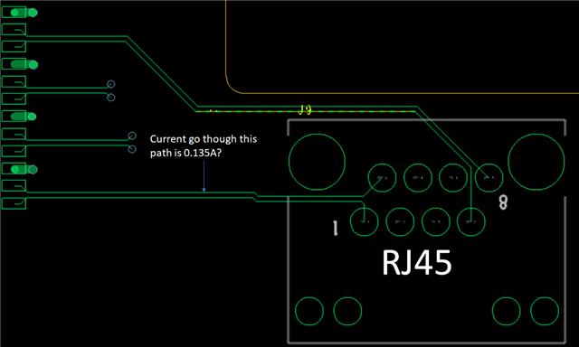
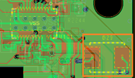
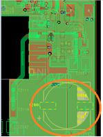
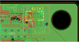
- D29 needs to be as close to the IC as possible. it should also have at least two vias per pad
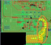
- the input power path is not optimized. The IC is on the opposite side of the board as the input. This is not preferred power path. The IC should be on the side of the transformer as the RJ45 input. We do want the IC pin DRAIN to be as close to the transformer as possible to minimize this path. It appears this is done. But we must also work to reduce the input power path in general.
- the input bulk cap should be closer to the IC as well.
- the drain path is too narrow. The entire primary side current is flowing through this trace, it should be bigger.
- Both RSNS resistors should have more vias
If this post answers your question, please indicate so by marking this thread as resolved. Thank you.