


Part Number: BQ76952
We work on the development of the high-power BMS design that consists of two boards:
- power board with MOSFETs + driver circuit
- logic board with BQ76952PFBR AFE
Currently, we created the first design of the power board using reference guide document "SLUAA84" as our design needs to have a low-side power switch. Please see attached schematic in PDF.
We received ready prototypes and during testing found some issues.
*** Correction ***
We tried to make a stand-alone operation for the power board as we haven't designed the logic board yet, so you can see added slider switches SW1,2. After first bring up we found that the voltage divider R94, R95 has not enough current capabilities as voltage does below the expected 6V when MOSFETs are ON. We removed this circuit and powered switches with an onboard 12V power supply (Q35 circuit).
After this correction, it seems that we able to open and close both sides of the MOSFET switch but when we apply load our boards get damaged. See our measurements:
**** Adding measurements ***
VIN = 22V
"12V" voltage regulator = 11.45V
1) Charge = OFF, Discharge = OFF
OUTPUT = 7.5V (slowly ramping down from ~10V to 7.5V each time we measure)
D-GATE = 0V
C-GATE = 0V
2) Charge = ON, Discharge = OFF
OUTPUT = 7.5V (slowly ramping down from ~10V to 7.5V each time we measure)
D-GATE = 0V
C-GATE = 10.8V
3) Charge = OFF, Discharge = ON
OUTPUT = 22V
D-GATE = 10.8V
C-GATE = 0V
4) Charge = ON, Discharge = ON
OUTPUT = 22V
D-GATE = 10.8V
C-GATE = 10V
Can you please help us to review the design and find any mistakes we could possibly make?
Thank you!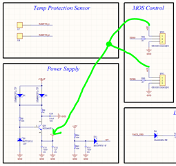
Schematic - BMS_PWR_REV1.0.PDF
