A related question is a question created from another question. When the related question is created, it will be automatically linked to the original question.
If you have a related question, please click the "Ask a related question" button in the top right corner. The newly created question will be automatically linked to this question.
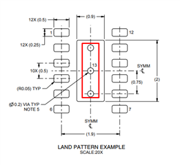
I am using the TPS62740 into my design. My appplication will consume just a few mA (5-10mA). Due to pcb area constraint I need to ommit the three vias recomended on the datasheet (pg 31). Is it ok?
From the electrical point of view, I don't see any concern about not placing the three vias on the thermal pad. But, please ensure the pad is connected to the GND pin (3) of the IC.
The primary purpose of the vias is to serve as a thermal relief by connecting the thermal pad of the IC to an internal GND plane of the PCB.
If based on your evaluation shows that the junction temperature (Tj) will not exceed 125 deg. C (allow at least 10% ~ 20% margin to accommodate the unit to unit variation) at worst-case conditions in your application, then removing the vias should be possible. Please refer to the formula below on how to calculate for the Tj with the WSON package.
Tj = Tc + (ψJT * Pdiss)
where:
Tc = case temperature
ψJT = junction-to-top characterization parameter (refer to the datasheet)
For the Pdiss_IC calculation, the inductor power and load switch losses need to be deducted to the input power as well. This is assuming a negligible power losses on input and output capacitors. By the way, the efficiency graph in the datasheet is only applicable if the load switch (pin #6) part of the IC is not used.
Pdiss_IC = Pin - Pout - (Ind_DCR x Iout) - (RLOAD * ILOAD)
where:
Ind_DCR: inductor maximum DC resistance
Iout: output current
RLOAD: high side MOSFET on-resistance
ILOAD: output current on Load Switch
Use a thermal camera or thermocouple (w/ temperature meter) to measure the case temperature of the device in actual application.