This thread has been locked.

If you have a related question, please click the "Ask a related question" button in the top right corner. The newly created question will be automatically linked to this question.

TPS62290: Load is too hot

Part Number: TPS62290

Dear Teams,

Could you help check following question from my customer?

Problem: As the power input VBUS dropped from 5V to about 2.2V, the output of TPS62290DRVT changed from normal 1.15V to about 2.9V, which caused serious load heating.

Experiment procedure:
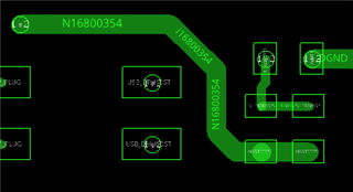
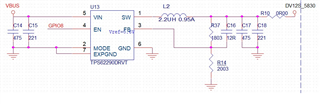
The circuit board uses TPS62290DRVT to supply power to a chip core, the power supply voltage is 1.15V, and the current is about 60mA. The chip itself has an LDO inside, and the measured voltage is about 1V, but the power consumption is relatively high, so an external DC-DC power supply is used to reduce power consumption.

VBUS is powered by the USB port of the computer. There is no problem with this circuit board directly plugged into the USB port. TPS62290DRVT can work normally, but the VBUS of this circuit board needs to be connected to another product, which needs to support hot plugging. The problem occurs in hot plugging. When pulling.
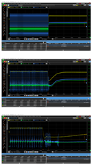
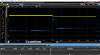
When this circuit board is inserted into another product, because this product has a larger starting current, the VBUS drops from 5V to about 2.2V, as shown in the figure below.

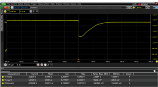
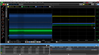
Due to the drop of VBUS, TPS62290DRVT began to work abnormally, and the voltage became about 2.9V, which caused the load current to directly increase to 600mA, and the chip became hot. After re-power on, all can work normally. The signal waveform of abnormal operation was measured with an oscilloscope. As shown in the figure below, the yellow line is VBUS, the green line is the output voltage 1.15V, and the blue line is the SW pin.

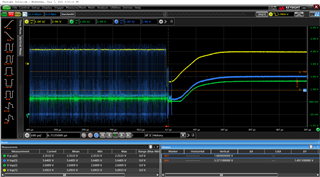
The minimum operating voltage given in the specification is 2.3V. We tested it with a switching power supply, and it stopped working at a minimum of 1.85V, but VBUS did not drop to 1.85V. Even if it is lower than 2.3V and does not work, and then VBUS rises again, it stands to reason that TPS62290DRVT should resume normal operation, but the result is like the waveform collected in the figure-the output voltage becomes 2.9V, SW pin There is no PWM wave anymore.
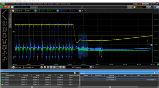
    After removing the load, the TPS62290DRVT is in light load mode, and the state of the SW pin is measured, as shown in the figure below. It is found that VBUS can work normally before it drops, and SW has a switching waveform after a period of time; after VBUS drops, the SW pin suddenly rises, then suddenly drops, and then slowly falls back, and no PWM wave is found. After a period of time, there is no PWM wave. It works normally again, there is no abnormal voltage, which is not the same as when there is a load 

So based on the results of the above measurement, I don’t understand why this phenomenon occurs. The drop of VBUS is a problem, but when there is a load and no load, what causes these two waveforms? ? ? Both of these phenomena present certain risks to users.

Thanks!

Dylan

  • Hi Dylan,

    Thanks for sharing all the details. I might need more clarity on a few things you explained above.

    1. From the schematic, I notice that you have used a lower input and output capacitance compared to what is recommended in the d/s for a stable operation.

    Also, considering the DC bias derating of capacitors, I believe this will be too less for input filtering. This device has strict input/output capacitance requirements.

    For stable operation, the L and C values of the output filter may not fall below 1-μH effective inductance and 3.5-μF effective capacitance. The part is optimized for operation with a 2.2-μH inductor and 10-μF output capacitor.

    What type of capacitors are used? Can you try to use higher capacitance?

    2. According to the measurements, I see that the VBUS drops to 2.2V for approx 20uS and takes more time to get back to normal values. This means it is also not operating in the recommended operating conditions of the IC which is not allowed.

    3. When powered using a USB port, I believe there is no voltage drop on VBUS and the device functions normally. Only when hot plugging the VBUS voltage drops.

    4. I could not spot any difference between the last two measurement plots. Can you please check?

    I am guessing that the device is not able to stabilize the loop and maintain the output voltage. I will review all details again and come back to you tomorrow.

    Regards,

    Febin

  • Hi Febin,

    1. The entire PCB is very small, about 26mmX13mm. VBUS has capacitors in other places. There are about 6 4.7uF/10V X5R ceramic capacitors on the entire PCB. The capacity should be no problem.
    2. VBUS will recover after about 200uS
    3. It is true that there is a load hot swap, which causes the VBUS to drop
    4. The last picture is the output waveform of TPS62290 when there is no load. When TPS62290 is no load, the output suddenly becomes the input voltage.
  • Hi Dylan,

    I went through all the details once again and could not deduce much from the above figures.

    - As a next step, could you please share the layout to see if we have missed out something crucial.

    - Also, it would be helpful if we could also look at the inductor current before the device enters 100% mode (with and without load). 

    - What I tried to ask earlier, about the last two pictures, the attached pictures looks the same with and without load. I assume you have attached wrong picture or was attached twice.  

    Let me confirm once again:

    With load=60mA:

    No load:

    Regards,

    Febin

  • The first three pictures is the waveform with load 60mA. The last one is with no load.

  • Hi Dylan,

    Thanks again. 

    1. Please share the layout if possible.

    2. Another test I would like to suggest is to measure VFB during the VIN drop. If the voltage is higher than 0.6V, then the Vout of TPS62290 might be supplied from an external circuit. You can check this by removing R10 and re-measuring Vout across C17/C18 during VIN drop. If the Vout is 1.15V, then there is no issue with TPS62290. And the output rail after R10 is supplied by another external source.

    Please let me know the results.

    Regards,

    Febin

  • Hi Febin,

    1. Please check the layout here P2 Pro V1_0 20210721.brd

    2. They already tested. It still has fault when they removed the R10. And the Vfb voltage is the voltage after voltage divider for Vout, then it will not maintain at 0.6V. Vfb will be greater than 0.6V.

    Thanks!

    Dylan

  • Hi Dylan,

    That's what I explained, if VFB>0.6V, then Vout is supplied from an external circuit. What is the Vout at this time?

    Please share the measurement plots including that for the inductor.

    Regards,

    Febin

  • Under no load condition, the Vout has been disconnected.

  • Hi Dylan,

    Unfortunately, I cannot understand the complete functioning of the system.

    Kindly share the below measurement plots to analyze further:

    1. Vin, Vout, SW, IL, EN, Vfb with R10 

    2. Vin, Vout, SW, IL, EN, Vfb without R10. 

    If you cannot replicate the Vin drop without R10, please use a schottky diode. I suppose the whole system will be functioning as normal even without R10. Adjust the feedback resistors to compensate for the diode voltage drop. 

    Meanwhile, I will review the layout and provide my feedback.

    Regards,

    Febin

  • Hi Dylan,

    Thank you for the call today. As explained in the call, below are my suggestions to improve the layout.

    1. You mentioned earlier that there are more capacitors on the board connected to VBUS. I could not find any additional capacitors close to U13 directly connected to the Vin of U13. The same for the output filter too. Which means the capacitance on the input & output side is below the d/s recommendations which may lead to unstable operation of this device.

    2. Feedback divider is connected on the top layer where as U13 is on the bottom (of a 6 Layer PCB). The feedback loop is connected using a long trace to the FB pin (also using multiple embedded vias) which is not recommended. It is better to have short & direct trace for this connection. The long traces may introduce noise and the Vout cannot be regulated.

    3. The GND planes in the layout also looks weak. For eg, the feedback resistor R14 is not connected to the GND pin, no proper GND connection for C14, C18, C17. Introduce more vias to efficiently dissipate heat to the underlying GND Layers. What I also see is that the bottom layer components are connected to GND1 and the top layer components are connected to GND2. And there is no connection between these GND planes. So I'm assuming all components of the buck are not having the same GND potential.

    4. The embedded vias under the thermal pad of the IC also contributes to additional noise. So by pulling the feedback network to the same layer as the IC, these vias can be eliminated.

    When an event like a Vin drop occurs, the current in the loop increases and there is high impedance in the GND connection causing more noise. This is why it is important to have a proper GND connection.

    Regards,

    Febin

  • Hi Febin,

    I just called customer about these suggestion.

    1. They have connected one 10uF capacitor on the input and output side via jumper wire. Therefore, the input and output capacitor should be more than 14.7uF, which is good in our recommendation region.

    2. They told me there is U6 TPS62290 with small FB trace in the PCB. And this IC also facing the same issue.

    4. They think this via has less effect on the event.

    U8 and U14 both are TPS62290 which convert to 2.8V and 3.3V separately.

    Thanks!

    Dylan

  • Hi Dylan,

    1. Can the customer solder directly at the input and output instead of C14 and C17.

    2. Can you mark on the layout where they connect the additional capacitors?

    3. Any updates on the scope plots? Please use clear and smaller scale (in uS).

    4. Does U8, U13, U14 have the same schematic? 

    5. Are all of them sharing the same VBUS?

    6. Please share more information on Hot Plugging of VBUS.

    7. What is the load for U8, U14? Is it also SoC?

    7. Does the Vin drop occur at all three devices simultaneously? If so, is the behaviour of all same? Please share the scope plots of all problematic devices.

    8. If I understand correctly, the device is not getting damaged after the event, but it only regulates at a different Vout (for eg. in U13 it is regulated at 2.9V after this event). After restarting the system, everything is normal.

    If something is unclear we can have a quick call.

    Regards,

    Febin

  • Hi Dylan,

    One more question:

    What is the ambient & junction temp of the IC during this Event?

    Regards,

    Febin

  • Hi Febin,

    Here is customer feedback:

    1. First of all, I think that if there is a problem with the capacitance value or the placement of the capacitor, then the chip may not work properly (for example, the ripple becomes larger), but the output voltage increases from 1.15V to 2.9V, which is very outrageous. (I have used Pin2Pin chips of the same package from other manufacturers, but this kind of abnormality did not appear)
    
    2. I directly connect C14 and C17 in parallel, I think it has little to do with the capacitor.
    
    3. I will adjust this, try to take a more detailed screenshot
    
    4. Yes, the same schematic diagram, but the feedback resistance is different, U6 is outputting 1.2V, U8 is outputting 2.8V, U13 is outputting 1.15V, U14 is outputting 3.3V
    
    5. Is sharing a VBUS
    
    6. You can take a small video and post it tomorrow
    
    7. I will measure this in detail tomorrow
    
    7. It was discovered that U6 and U13 had problems. U14's output voltage of 3.3V only dropped briefly and returned to normal soon. U8 did not measure
    
    8. The power supply for the core of this Soc is around 1.1V, and a voltage of 2.9V makes the chip very hot, and the power is cut off quickly. If the power is uninterrupted, Soc will be burned, because U13 has not recovered to the normal power supply voltage. In addition, although the output voltage of U6 increased at first and then recovered to 1.2V, it may still cause damage to my Soc.
    9. The ambient temperature is 25 degree c.
    
    In addition, can I use other equipment to simulate the drop of VBUS? I have used two 47 ohm resistors in parallel with the load under this kind of VBUS drop condition, and this kind of abnormal phenomenon has also occurred. You can try it.
  • Hi Dylan,

    Please send me the results of the new measurements internally and we will continue the conversation there.

    Regards,
    Davor