This thread has been locked.

If you have a related question, please click the "Ask a related question" button in the top right corner. The newly created question will be automatically linked to this question.

LM2733: LM2733XMFX/NOPB Current Consumption Issue

Part Number: LM2733

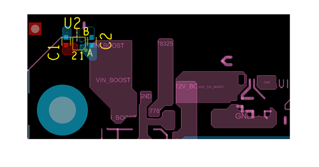
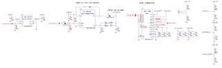
We are using LM2733 in our design with input coming from battery also in LM2733 shutdown mode there will be some leakage from inductor and diode path so we are using load switch before LM2733 boost regulator.

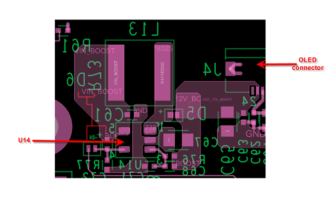
At the load side of boost regulator we have 1.54" OLED which has current consumption of 50mA maximum.

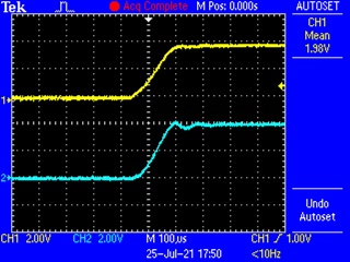
When we check current at battery terminals with OLED on it shows current consumption of 350mA which is too much.

Earlier we we were using MPS boost regulator MP3437 and the current consumption was only 20mA which has been increased after using LM2733 to 350mA.

Kindly advise if we are missing anything here.

Please note netname SW_BOOST_EN & EN_BOOST_12V are connected to STM32 MCU.

  • Hi Adil,

    what is the input voltage and output voltage when see 350mA input current?

    if the output current is 50mA, how is it possible to see only 20mA from the input? the input energy must be higher than output energy. 

  • Hi Jasper,

    Kindly find details below:

    Input Voltage: Li-Ion Battery Voltage (3V to 4.2V)

    Output Voltage: 12V

    Load we have: LCD Operating at 12V with Current Consumption of 35mA maximum

    Issue:

    When we turn on LCD we get consumption of 350mA at input which should be maximum 180mA because (12Vx35mA)/3.7V=113mA. After efficiency factor it should be like maximum 180mA consumption at battery when we have only load of LM2733 which is supplying to LCD only.

  • Can you please review attached circuit and advise if we can do anything to improve this current consumption factor or anything you find fishy in the circuit. Please advise

  • Hi Adil,

    i don't issue from the schematic. 

    1. Did you confirm the same issue in several boards. make sure this is not caused by soldering issue.

    2. please measure the VIN and VOUT waveform when seeing 350mA

  • Hi Jasper, 

    We are seeing this on multiple boards. I will share waveforms shortly. 

  • Here are some debugging we did:

    Case0: OLED populated, turned ON U2 and U14 [current: ~450mA]

    Case1: Turned OFF OLED from MCU, turned ON U2 and U14 [current: ~450mA]

    Case2: Physically removed OLED display, turned ON U2 and U14 [current: ~450mA]

    Case3: Isolated EN_BOOST_12V from ST MCU by removing D6, turned on U2 and enabled U14 with via jumper [current: ~450mA]

    Case4: Removed U2, enabled U14 via jumper, provided VIN_BOOST with a jumper from VBAT to C61.1 [current: 450mA]

    The VOUT is same as VBAT. 

  • Hi Adeel,

    it seem the IC is damaged if there is not loading in the output of the boost.

    please check the impedance of each pins to GND pin. and what happen if the BOOST is disabled?

  • Hi Jasper, 

    Please see attached waveforms. CH#1 is connected to VIN_BOOST at C61 and CH#2 is connected to VCC_12V_BOOST at C67. From the waveforms we don't see any switching behavior .These waveforms are verified on two boards by two independent EE engineers. During this time VBAT was 3.92V. 


    Checking Resistance Btw each Pin and GND when BOOST in enabled. 

    PIN#5 to GND: 0.5M Ohms
    PIN#4 to GND: 120K Ohms
    PIN#3 to GND : 12K Ohms
    PIN#2----> GND PIN
    PIN#1 to GND: 0.5M Ohms

    Is there a way to verify that the IC is not damaged ? We have ordered eval kits for LM2733Y ( LM2733X eval kit is not available on TI website) for further testing. 

  • Adeel,

    from these impedances, it is hard to say the IC damaged or not. you can change the board with a fresh new IC and measure the impedance again.

    as pin resistor is not much small, where does the 450mA go?

    did you measure the waveform of SW, EN and FB pin? 

    also please the layout image.

  • I am not sure where is the 450mA flowing. Please see layout pictures. 

    I will share SW, EN,and FB waves tomorrow.


  • Adeel,

    the layout looks OK. 

    is the IC very hot? if not, which components is hot. from closed to 4V input, the total power loss is 1.8W. this is not small power loss.

    also you can try to disconnect the loading if possible